
CMOS Logic Gate Principles
Enroll to start learning
You’ve not yet enrolled in this course. Please enroll for free to listen to audio lessons, classroom podcasts and take practice test.
Interactive Audio Lesson
Listen to a student-teacher conversation explaining the topic in a relatable way.
Basic CMOS Logic Gate Structure
🔒 Unlock Audio Lesson
Sign up and enroll to listen to this audio lesson

Today, we will explore the basic structure of CMOS logic gates. Can anyone tell me what types of transistors are used in these gates?

Are they NMOS and PMOS transistors?
Correct! The NMOS conducts when the gate-source voltage is positive, while the PMOS conducts when it's negative. This complementary action minimizes static power consumption. Why is that important?

Because it saves energy! Only one transistor is on at a time!
Exactly! This allows CMOS gates to be more power-efficient, which is crucial for devices like microprocessors. Let's remember this with the mnemonic: 'Only One Active'—it highlights that only one transistor is active at any time. Now, could anyone explain what happens at the output based on the input?

If the input is high, NMOS pulls the output to low or ground. If low, PMOS pulls it to high.
Well done! That leads us to understanding the function of the inverter, the simplest CMOS gate.
The CMOS Inverter
🔒 Unlock Audio Lesson
Sign up and enroll to listen to this audio lesson

The CMOS inverter is fundamental in logic design. Can someone explain its structure?

It has a PMOS connected to Vdd and an NMOS connected to ground.
Good job! Now, how does it operate when the input is high?
When the input is high, NMOS turns on and pulls the output to low.
That's correct. Conversely, what happens when the input is low?
The PMOS turns on, pulling the output to high.
Exactly! Let's summarize the truth table of the inverter. Who wants to read it out loud?
"| Input (Vin) | Output (Vout) |
NAND and NOR Gates
🔒 Unlock Audio Lesson
Sign up and enroll to listen to this audio lesson
Moving beyond the inverter, let's discuss NAND and NOR gates. Who can tell me what it means for a gate to be 'universal'?
It means they can create any logic function.
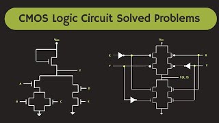
Exactly! A NAND gate has two NMOS transistors in series and two PMOS transistors in parallel. What do you think happens when both inputs are high?
Then both NMOS turn on, pulling the output low.
Correct! And in the other cases, what does the output do?
It goes high because at least one PMOS would turn on.
Exactly! Let's review the truth table for the NAND gate briefly. Can someone summarize it?
"| A | B | Output |
Introduction & Overview
Read summaries of the section's main ideas at different levels of detail.
Quick Overview
Standard
This section delves into the principles of CMOS logic gates, highlighting basic gate structures, such as inverters, NAND, and NOR gates. It emphasizes their operational behavior, truth tables, and the advantages of using complementary transistors for efficient logic design.
Detailed
CMOS Logic Gate Principles
CMOS logic gates form the backbone of digital circuits and are constructed using complementary transistors: NMOS and PMOS. In a basic CMOS structure, the NMOS transistor conducts when the input is high, while the PMOS transistor conducts when the input is low. This complementary action minimizes static power consumption, ensuring only one transistor conducts at any time.
Basic CMOS Logic Gate Structure
A typical CMOS logic gate includes two types of transistors:
- NMOS Transistor: Conducts and pulls the output to ground when the input is high (1).
- PMOS Transistor: Conducts and pulls the output to Vdd (supply voltage) when the input is low (0).
The output voltage is driven to Vdd or ground based on the input state, showcasing the efficient power management of CMOS technology.
The CMOS Inverter
The simplest form of a logic gate in CMOS is the inverter, which inverts an input signal:
- Structure: Consists of PMOS transistor linked to Vdd and NMOS connected to ground, sharing a drain node for output.
- Operation: When the input is high, NMOS conducts (output low), while PMOS is off. Conversely, when the input is low, PMOS conducts (output high).
Truth Table of the CMOS Inverter
| Input (Vin) | Output (Vout) |
|---|---|
| 0 | 1 |
| 1 | 0 |
Understanding these principles lays the foundation for more complex gates like NAND and NOR, which are marked as universal gates, crucial in constructing various logical functions.
Youtube Videos


Audio Book
Dive deep into the subject with an immersive audiobook experience.
Basic CMOS Logic Gate Structure
Chapter 1 of 3
🔒 Unlock Audio Chapter
Sign up and enroll to access the full audio experience
Chapter Content
A CMOS logic gate consists of two transistors of complementary types:
- NMOS transistor: Conducts when the gate-source voltage (VGSV_{GS}) is positive, typically when the input is high (1).
- PMOS transistor: Conducts when the gate-source voltage is negative, typically when the input is low (0).
The complementary action of these transistors ensures that:
- One transistor is on while the other is off, minimizing static power consumption.
- The output voltage will be driven either to the supply voltage (for PMOS) or to ground (for NMOS), based on the input.
Detailed Explanation
A CMOS logic gate is a combination of two types of transistors: NMOS and PMOS. The NMOS transistor conducts electrical current when its input signal is high, while the PMOS transistor does so when its input signal is low. Because only one of these transistors is on at a time, this design significantly reduces power consumption when the logic gate is not switching states. The output of the gate will either connect to the power supply (when the PMOS is on) or to ground (when the NMOS is on), depending on the input signal's state.
Examples & Analogies
Imagine a pair of light switches arranged so that only one can be 'on' at any time. When you flip one switch up (turning on the light), the other switch must flip down (turning off the light). This setup is similar to how NMOS and PMOS transistors operate; they work together to control the flow of electricity depending on the signals they receive.
The CMOS Inverter
Chapter 2 of 3
🔒 Unlock Audio Chapter
Sign up and enroll to access the full audio experience
Chapter Content
The simplest CMOS logic gate is the inverter, which performs the NOT operation by inverting the input signal.
- Structure: The CMOS inverter consists of a PMOS transistor connected to Vdd (positive supply) and an NMOS transistor connected to ground. The input signal is fed to the gates of both transistors, and the output is taken from the common drain node.
- Operation:
- When the input is high (1), the NMOS transistor turns on, pulling the output to low (0). The PMOS transistor is off.
- When the input is low (0), the PMOS transistor turns on, pulling the output to high (1). The NMOS transistor is off.
Detailed Explanation
The CMOS inverter is a specific type of logic gate that effectively reverses the input signal. In its basic structure, a PMOS transistor is connected to the positive supply voltage (Vdd), and an NMOS transistor is connected to ground. If the input is a high signal (1), the NMOS transistor allows current to flow to ground, making the output low (0). Conversely, if the input is low (0), the PMOS transistor allows current to flow from the positive supply to the output, making it high (1). This dual-action is what makes the inverter function as a NOT gate.
Examples & Analogies
Think of a simple toggle switch: when you flip it one way (high or 1), the light turns off (output 0), and when you flip it the other way (low or 0), the light turns on (output 1). The inverter works in exactly the same way, flipping the input to give the opposite output.
Truth Table of the CMOS Inverter
Chapter 3 of 3
🔒 Unlock Audio Chapter
Sign up and enroll to access the full audio experience
Chapter Content
Input Output
(VinV_{in}) (VoutV_{out})
0 1
1 0
Detailed Explanation
The truth table for the CMOS inverter summarizes its operation. It shows the relationship between the input and output signals. If the input (Vin) is 0, the output (Vout) will be 1. Conversely, if the input is 1, the output will be 0. This inversion illustrates the fundamental behavior of the NOT operation performed by the inverter.
Examples & Analogies
Imagine a door with a mechanism that automatically locks when open (input 1) and unlocks when closed (input 0). The door's status reflects the opposite of its position just like the inverter reflects the opposite value of the input signal.
Key Concepts
-
CMOS Logic Gates: Built using NMOS and PMOS transistors for efficient operation.
-
NAND and NOR Gates: Universal gates that can implement any logic function.
-
Inverter Function: A fundamental CMOS gate that inverts the input signal.
Examples & Applications
An inverter circuit where the output is the logical negation of the input signal.
A NAND gate configured to perform a specific logic function within a larger digital circuit.
Memory Aids
Interactive tools to help you remember key concepts
Rhymes
NMOS pulls down, PMOS pulls up, In a gate, they form a power cup.
Stories
Imagine two friends playing tug-of-war in a logic game—one pulls down when the other isn't smiling, showcasing the inverter’s functionality.
Memory Tools
NMOS/Never Miss Output Salve, PMOS/Pulls More On Switch- It helps to remember transistor behaviors.
Acronyms
NAND - Not AND, remember—only one high keeps it in the game!
Flash Cards
Glossary
- CMOS
Complementary Metal-Oxide-Semiconductor, a technology for constructing integrated circuits using complementary and asymmetrical pairs of p-type and n-type MOS transistors.
- NMOS
A type of MOSFET (Metal-Oxide-Semiconductor Field-Effect Transistor) that uses n-type semiconductor material; used in low-side switching.
- PMOS
A type of MOSFET that uses p-type semiconductor material; used in high-side switching.
- Inverter
A logic gate that outputs the opposite value of its input (NOT gate).
- NAND Gate
A digital logic gate that outputs false only when all its inputs are true.
- NOR Gate
A digital logic gate that outputs true only when all its inputs are false.
Reference links
Supplementary resources to enhance your learning experience.