
Digital CMOS Logic Design - Part 1: Principles of Digital CMOS Logic Gates
Enroll to start learning
You’ve not yet enrolled in this course. Please enroll for free to listen to audio lessons, classroom podcasts and take practice test.
Interactive Audio Lesson
Listen to a student-teacher conversation explaining the topic in a relatable way.
Introduction to Digital CMOS Logic Gates
🔒 Unlock Audio Lesson
Sign up and enroll to listen to this audio lesson

Welcome, everyone! Today, we're diving into the world of digital CMOS logic gates. Can anyone explain what CMOS stands for?

I believe it stands for Complementary Metal-Oxide-Semiconductor.
Exactly! CMOS technology is fundamental because it uses both NMOS and PMOS transistors. What can you tell me about the advantages of using CMOS technology?

CMOS gates consume less power because only one transistor conducts at a time, right?
Exactly, that's a crucial point. It allows for more efficient designs. Let's remember that: 'One conducts, one rests.'

So they can be integrated tightly on a chip?
Yes! Integration allows for more complex designs. To summarize, CMOS technology enables low power consumption and high integration. Any questions before we proceed?
Working of the CMOS Inverter
🔒 Unlock Audio Lesson
Sign up and enroll to listen to this audio lesson

Let’s focus on the CMOS inverter, a fundamental gate. Can someone describe its structure?

It has a PMOS transistor connected to Vdd and an NMOS connected to ground.
Correct! So, what happens when we input a high signal?
The NMOS turns on, and the output goes low.
Exactly! When the input is low, the PMOS turns on, and the output goes high. Let’s recap that: High input leads to low output, and low input leads to high output. It’s like a flip! Can you guys tell me what that is in table form?
It's a truth table! 0 leads to 1 and 1 leads to 0.
Awesome! Let’s summarize the inverter's function and its importance in CMOS technology.
NAND and NOR Gate Operations
🔒 Unlock Audio Lesson
Sign up and enroll to listen to this audio lesson
Now, let’s explore NAND and NOR gates. Who recalls what universal gates mean?
They can be used to create any type of logic function!
Good point! The NAND gate outputs low only when both inputs are high. How does that work?
The NMOS turns on when inputs are high and the output goes low.
Exactly! Now, what about the NOR gate? What’s its operation?
The NOR gate outputs high only when both inputs are low.
Correct! Both gates are vital components. Any questions about their truth tables?
XOR and XNOR Gate Applications
🔒 Unlock Audio Lesson
Sign up and enroll to listen to this audio lesson
Next, we focus on XOR and XNOR gates. Can anyone summarize the XOR operation?
It outputs high when the inputs differ!
Exactly! Now how about the XNOR gate? What does it do?
It outputs high when the inputs are the same!
Great! These gates are crucial for tasks like parity checking. Let's take a moment to consolidate this: XOR is useful for detecting difference, while XNOR is for verifying similarity. Any questions?
Performance Metrics
🔒 Unlock Audio Lesson
Sign up and enroll to listen to this audio lesson
To wrap up, let’s discuss performance metrics of CMOS gates. What is propagation delay?
It's the time it takes for an input change to influence the output.
Exactly! Can you think of factors that might influence this delay?
Transistor size and capacitance definitely play a role.
Correct! Now, what about power consumption?
CMOS has low static power consumption but can have dynamic power when switching.
Very good! Remember, understanding noise margins is also essential, as they show how much noise a gate can tolerate. To summarize: we covered propagation delay, power consumption, and noise margins. Great work, everyone!
Introduction & Overview
Read summaries of the section's main ideas at different levels of detail.
Quick Overview
Standard
The section provides a detailed exploration of digital CMOS logic gates, focusing on fundamental gates such as inverters, NAND, NOR, XOR, and XNOR gates. It discusses their structures, operational principles, truth tables, performance metrics like propagation delay and power consumption, and design considerations in CMOS technology.
Detailed
Digital CMOS Logic Design - Principles of Digital CMOS Logic Gates
Introduction
Digital logic gates are essential components in modern electronics, notably in microprocessors and communication systems. CMOS technology utilizes complementary NMOS and PMOS transistors for creating efficient logic gates with low power consumption.
CMOS Logic Gate Principles
Basic Structure
A CMOS logic gate comprises NMOS and PMOS transistors that work complementarily to minimize power use.
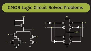
CMOS Inverter
- Functionality: Converts an input signal to its opposite.
- Truth Table:
- Input 0 → Output 1
- Input 1 → Output 0
NAND and NOR Gates
Both gates serve as universal gates—capable of constructing any digital logic circuit.
- NAND Gate:
- Outputs low only when both inputs are high.
- NOR Gate:
- Outputs high only when both inputs are low.
XOR and XNOR Gates
These gates are more complex designs used for operations like parity checking. XOR outputs high when inputs differ, while XNOR outputs high when inputs are the same.
Performance Metrics
Considerations include propagation delay, dynamic power consumption related to capacitance, and noise margin to measure robustness against signal variations.
Summary
CMOS logic gates are pivotal in digital circuits. Key metrics—like propagation delay and power use—are vital in their design and application.
Youtube Videos


Audio Book
Dive deep into the subject with an immersive audiobook experience.
Introduction to CMOS Logic Gates
Chapter 1 of 4
🔒 Unlock Audio Chapter
Sign up and enroll to access the full audio experience
Chapter Content
Digital logic gates are the fundamental building blocks of digital circuits used in modern electronics, including microprocessors, memory systems, and communication systems. In CMOS technology, digital logic gates are designed using CMOS transistors—complementary NMOS and PMOS devices. These gates provide the necessary functionality to perform logical operations (such as AND, OR, NOT, XOR, etc.) by processing binary signals (0s and 1s). The primary advantage of CMOS digital logic gates is their low power consumption, as only one transistor is typically conducting at any time in a complementary configuration. Additionally, CMOS technology allows for the integration of a large number of logic gates on a single chip, enabling the development of complex digital systems. In this chapter, we explore the basic principles and design of CMOS digital logic gates, starting with the simplest gate, the inverter, and expanding to more complex gates such as NAND, NOR, XOR, and XNOR.
Detailed Explanation
Digital CMOS logic gates are essential components in creating electronic circuits. They process binary signals, where a '0' can represent low voltage and '1' can represent high voltage. CMOS, which stands for Complementary Metal-Oxide-Semiconductor, utilizes two types of transistors: NMOS and PMOS, which work together. One key benefit of CMOS technology is its efficiency; only one type of transistor operates at a time, reducing power consumption. This technology also enables compact designs, leading to complex circuits like those found in modern microprocessors.
Examples & Analogies
Think of CMOS logic gates like a light switch in your home. When you turn on a light, you create a pathway for electricity to flow, similar to how a transistor conducts when activated. However, only one switch (transistor) is active at a time, ensuring the rest of the house remains energy-efficient—just as CMOS technology minimizes power use in electronics.
Basic CMOS Logic Gate Structure
Chapter 2 of 4
🔒 Unlock Audio Chapter
Sign up and enroll to access the full audio experience
Chapter Content
A CMOS logic gate consists of two transistors of complementary types:
● NMOS transistor: Conducts when the gate-source voltage (VGS) is positive, typically when the input is high (1).
● PMOS transistor: Conducts when the gate-source voltage is negative, typically when the input is low (0).
The complementary action of these transistors ensures that:
● One transistor is on while the other is off, minimizing static power consumption.
● The output voltage will be driven either to the supply voltage (for PMOS) or to ground (for NMOS), based on the input.
Detailed Explanation
In the structure of a CMOS logic gate, two types of transistors are used: NMOS and PMOS. The NMOS transistor turns on (conducts) when the input signal is high, allowing current to flow. Conversely, the PMOS transistor activates when the input is low. This complementary functionality is significant because it guarantees that at any given moment, only one type of transistor is conducting, which reduces energy wastage. Depending on which transistor is active, the output can either be high (connected to the power supply through PMOS) or low (connected to ground through NMOS).
Examples & Analogies
Imagine a see-saw in a playground: when one side is up, the other side is down. In the same way, in a CMOS gate, when one transistor (like one end of the see-saw) is 'on' and conducting, the complementary transistor is 'off' and not conducting. This balance ensures safety and efficiency, just as the see-saw operates better when one side is not too heavy.
The CMOS Inverter
Chapter 3 of 4
🔒 Unlock Audio Chapter
Sign up and enroll to access the full audio experience
Chapter Content
The simplest CMOS logic gate is the inverter, which performs the NOT operation by inverting the input signal.
● Structure: The CMOS inverter consists of a PMOS transistor connected to Vdd (positive supply) and an NMOS transistor connected to ground. The input signal is fed to the gates of both transistors, and the output is taken from the common drain node.
● Operation:
○ When the input is high (1), the NMOS transistor turns on, pulling the output to low (0). The PMOS transistor is off.
○ When the input is low (0), the PMOS transistor turns on, pulling the output to high (1). The NMOS transistor is off.
Detailed Explanation
The CMOS inverter is the most basic type of logic gate, performing the NOT function. It consists of a PMOS transistor connected to the positive voltage supply and an NMOS transistor connected to ground, with both sharing a common output connection. If the input signal is high (logical '1'), the NMOS turns on and pulls the output down to zero (low). When the input is low (logical '0'), the PMOS turns on, driving the output to the supply voltage (high). This means the output is always the logical opposite of the input.
Examples & Analogies
Consider a light switch that can either be in the 'on' or 'off' position. The inverter works the same way: when you turn the switch on, the light (output) turns off, and vice versa. It’s like flipping a coin; if heads is on the table, tails is the opposite side facing up, readily showing you that only one can face up at a time.
Truth Table of the CMOS Inverter
Chapter 4 of 4
🔒 Unlock Audio Chapter
Sign up and enroll to access the full audio experience
Chapter Content
Input (Vin) | Output (Vout)
0 | 1
1 | 0
Detailed Explanation
The truth table of the CMOS inverter summarizes its operation. It lists possible input values alongside the corresponding output values. For an input of '0', the output is '1', meaning it's in the 'on' state. Conversely, if the input is '1', the output is '0', meaning the output is 'off'. This clear relationship shows how the inverter functions to invert signal levels effectively.
Examples & Analogies
Think of the ASCII characters for digital signals: if '0' is like being asleep (inactive), then the output '1' represents waking up (active). Whenever the input signal changes, the inverter flips that state, akin to a person who instantly wakes up or goes back to sleep depending on the noise—this demonstrates the on/off dynamic clearly.
Key Concepts
-
CMOS Technology: A method of fabricating integrated circuits using complementary pairs of p-type and n-type transistors.
-
Logic Gates: Fundamental building blocks that perform logical operations on binary inputs.
-
Inverter: A basic CMOS gate that outputs the inverse of its input.
-
NAND Gate: A gate that outputs false only when all inputs are true.
-
NOR Gate: A gate that outputs true only when all inputs are false.
-
XOR Gate: Outputs true when inputs differ.
-
XNOR Gate: Outputs true when inputs match.
-
Propagation Delay: Key metric indicating the responsiveness of the gate.
-
Power Consumption: Assessment of energy use in CMOS circuits.
Examples & Applications
The CMOS inverter can transform a logical 1 into a 0 and vice versa, typically used in digital circuits to perform NOT operations.
NAND and NOR gates can be combined to create more complex logic functions, showcasing their universality in digital design.
Memory Aids
Interactive tools to help you remember key concepts
Rhymes
In CMOS, one rests, the other conducts, keep it low; power consumption reduces, that's how the circuits grow!
Stories
Imagine a city with two roads: the NMOS road is bustling only when it rains (input high), while the PMOS road is quiet unless the sun shines (input low). Together, they lead traffic efficiently - that's how inverters work!
Memory Tools
NAND: Not And, means it’s false only when true; NOR: Not Or, is high only if both inputs are blue.
Acronyms
For XOR, remember ‘ODD’ – outputs high for Odd (1 or 3 true inputs); and for XNOR, remember ‘EVERY’ – EVERY input must match for a high output.
Flash Cards
Glossary
- CMOS
Complementary Metal-Oxide-Semiconductor technology used for constructing integrated circuits.
- NMOS
N-type Metal-Oxide-Semiconductor; it conducts when a positive voltage is applied.
- PMOS
P-type Metal-Oxide-Semiconductor; it conducts when a negative voltage is applied.
- Inverter
A logic gate that outputs the opposite value of the input.
- NAND Gate
A universal gate that outputs low only when all its inputs are high.
- NOR Gate
A universal gate that outputs high only when all its inputs are low.
- XOR Gate
A digital gate that outputs high when an odd number of inputs are high.
- XNOR Gate
A digital gate that outputs high when even numbers of inputs are high.
- Propagation Delay
The time it takes for an input change to propagate through a gate to affect the output.
- Power Consumption
The amount of power used by a digital circuit during operation.
Reference links
Supplementary resources to enhance your learning experience.