
CMOS NAND Gate
Enroll to start learning
You’ve not yet enrolled in this course. Please enroll for free to listen to audio lessons, classroom podcasts and take practice test.
Interactive Audio Lesson
Listen to a student-teacher conversation explaining the topic in a relatable way.
Structure of the CMOS NAND Gate
🔒 Unlock Audio Lesson
Sign up and enroll to listen to this audio lesson

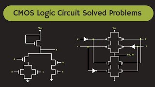
Let’s dive into the structure of the CMOS NAND gate. It combines two NMOS transistors in series and two PMOS transistors in parallel. Can anyone tell me what 'NMOS' and 'PMOS' refer to?

I think NMOS stands for N-type Metal-Oxide-Semiconductor, and PMOS is for P-type.
Exactly right! This complementary structure ensures that when both NMOS are ON, the output goes to ground. What happens if one input is low?

Then at least one PMOS turns on, which keeps the output high!
Great observation! This complementary action minimizes power consumption as well. Now, how would you describe the output when both inputs are high?

The output would be low, as both NMOS will conduct.
Correct! To summarize, the NAND gate structure is pivotal in digital circuits as it allows for a low output only when both inputs are high.
Operation of the CMOS NAND Gate
🔒 Unlock Audio Lesson
Sign up and enroll to listen to this audio lesson

Now, let’s delve into the operation of the CMOS NAND gate. Can someone explain what the output is when both inputs are at 1?

The output is 0.
Right! And what about when both inputs are at 0?
The output would be 1!
Exactly! This truth table shows how versatile the NAND gate is. It can yield a high output unless both inputs are high. Can anyone think of a practical application for this?
Using NAND gates to create other logic circuits, like flip-flops or latches!
Awesome! To wrap up, the NAND gate is a foundational building block in digital design, allowing for creative constructions of complex logic functions.
Truth table and significance of the NAND Gate
🔒 Unlock Audio Lesson
Sign up and enroll to listen to this audio lesson
Now let's look closely at the truth table for the NAND gate. Can anyone share what the truth table looks like?
For inputs (0, 0), (0, 1), and (1, 0), the output is 1, and for (1, 1), the output is 0.
Perfect! This means the NAND gate is high for any combination of input, except when both inputs are high. Why do you think this property is significant?
Because it allows us to create any other logic gate! The NAND gate is universal.
Correct! The universal property of the NAND gate makes it incredibly powerful in circuit design. Could you list why simplicity is valuable in designing circuits?
Fewer components mean reduced costs and complexity in troubleshooting.
Exactly! The NAND gate's efficiency is a prime reason for its widespread use. Remember, this gate is not just useful on its own but serves as the basis for building more complex systems.
Introduction & Overview
Read summaries of the section's main ideas at different levels of detail.
Quick Overview
Standard
The CMOS NAND gate is constructed using electronic components known as NMOS and PMOS transistors. This section explains its operation — how the gate functions based on different combinations of inputs — and presents its truth table, emphasizing its role as a universal gate capable of implementing any logical function.
Detailed
Detailed Summary of CMOS NAND Gate
The CMOS NAND gate is a crucial digital component constructed from complementary NMOS and PMOS transistors. Its design incorporates two NMOS transistors connected in series and two PMOS transistors connected in parallel. The functionality of the NAND gate arises from the behavior of these transistors:
- Operation of the NAND Gate:
-
When both inputs are set high (
1), the series NMOS transistors activate, delivering a low output (0). In contrast, if either or both inputs are low (0), at least one PMOS transistor activates, resulting in a high output (1). This complementary action is central to the NAND gate’s functionality. - Truth Table: The truth table for the NAND gate illustrates how the output signal varies based on the input combinations:
- For input states
(0, 0),(0, 1), and(1, 0), the output is high (1). Only when both inputs are high (1, 1) does the output fall to low (0). The visualization of these states reinforces how NAND gates offer versatile applications in digital logic due to their ability to condense multiple inputs into a controlled output.
Understanding the NAND gate is essential for grasping advanced topics in digital electronics, as it serves as a basis for constructing all other types of logic gates and circuits.
Youtube Videos


Audio Book
Dive deep into the subject with an immersive audiobook experience.
Introduction to the CMOS NAND Gate
Chapter 1 of 2
🔒 Unlock Audio Chapter
Sign up and enroll to access the full audio experience
Chapter Content
The CMOS NAND gate is made by connecting two NMOS transistors in series and two PMOS transistors in parallel. The NMOS transistors pull the output to ground when both inputs are high, while the PMOS transistors pull the output to Vdd when at least one input is low.
Detailed Explanation
The CMOS NAND gate's structure consists of two key components: NMOS transistors and PMOS transistors. The NMOS transistors are connected in series, meaning that both must be 'on' (conducting) for the output to be pulled down to ground (0). Conversely, the PMOS transistors are in parallel, which means at least one must be 'on' (conducting) to pull the output up to the positive supply voltage (Vdd). This design allows the NAND gate to output a high signal (1) for most input combinations, except when both inputs are high.
Examples & Analogies
Think of a NAND gate like a light switch with two switches. If both switches are off, the light is on (output is high); however, if both switches are on, the light turns off (output is low). This gate's operation is akin to ensuring that you only get the light on if not both conditions are met.
Operation of the CMOS NAND Gate
Chapter 2 of 2
🔒 Unlock Audio Chapter
Sign up and enroll to access the full audio experience
Chapter Content
● Operation:
○ When both inputs are high (1), both NMOS transistors turn on, pulling the output to low (0). Both PMOS transistors are off.
○ In all other cases (one or both inputs are low), the output will be high (1) due to the complementary action of the PMOS transistors.
Detailed Explanation
In operation, the CMOS NAND gate behaves dependently on its inputs. If both inputs are high (1), the NMOS transistors activate, creating a path to ground and thus making the output low (0). If either or both inputs are not high (i.e., they are low or 0), the PMOS transistors will create a connection to Vdd, resulting in a high output (1). This characteristic demonstrates the 'NAND' functionality—outputting low only when both inputs are high.
Examples & Analogies
Imagine a security system in a house where two locks must both be engaged for the alarm to be disabled. If both locks are engaged (both inputs high), the alarm will not go off (output low). However, if either lock is not engaged (one or both inputs low), the alarm remains off (output high). This way, the security system protects the house by not allowing disarming unless both conditions are satisfied.
Key Concepts
-
CMOS NAND Gate: A digital logic gate that produces an output of low only when all inputs are high.
-
Universal Gate: A logic gate that can be used to create any other logic gate, including AND, OR, etc.
-
Input Combinations: The various states of inputs which determine the output based on the gate's defined logic.
Examples & Applications
Example of a NAND Gate: If we input (1, 0) into a NAND gate, the output will be 1.
Practical Use: NAND gates are used in building memory devices like SRAM and flash memory.
Memory Aids
Interactive tools to help you remember key concepts
Rhymes
NAND's the gate that says no to both, but yes to one, a logic classic in electronic fun!
Stories
In a digital world, two inputs meet at a gate. They dance, and if both are up, down they go in a low state, but if at least one dips, the output gives a lift!
Memory Tools
NAND: Negate AND, so remember - 'Not And!' helps you recall its unique command.
Acronyms
NAND
- Not
- And
- Not
- Again.
Flash Cards
Glossary
- CMOS
Complementary Metal-Oxide-Semiconductor; a technology for constructing integrated circuits, including logic gates.
- NAND Gate
A universal digital logic gate that outputs low only when all its inputs are high.
- NMOS Transistor
A type of transistor that conducts when the gate voltage is high; allows current to flow when activated.
- PMOS Transistor
A type of transistor that conducts when the gate voltage is low; allows current to flow when activated.
- Truth Table
A table that lists all possible input combinations of a logic gate and their corresponding outputs.
Reference links
Supplementary resources to enhance your learning experience.