
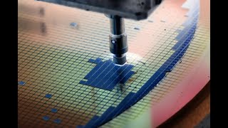
ALD Deposition Cycle
Interactive Audio Lesson
Listen to a student-teacher conversation explaining the topic in a relatable way.
Introduction to ALD
🔒 Unlock Audio Lesson
Sign up and enroll to listen to this audio lesson

Today we're diving into Atomic Layer Deposition, or ALD. Does anyone know what it is?

Is it a method of depositing thin films?
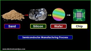
Exactly! ALD is a process used to deposit thin films one monolayer at a time. This is crucial in fields like semiconductor manufacturing where precision is key.

Why is it important to deposit just one layer at a time?
Great question! Depositing one layer at a time allows for atomic-level control over the film thickness, which is essential for creating devices like transistors.

So, how does the process actually work?
Let's discuss the steps involved in the ALD cycle. It consists of four key steps.
Steps of the ALD Cycle
🔒 Unlock Audio Lesson
Sign up and enroll to listen to this audio lesson

In the ALD cycle, the first step is the exposure to Precursor A. This is where the chemical vapor interacts with our substrate. Student_4, can you tell us what happens next?

After that, we purge it to get rid of any leftover chemicals, right?
Exactly! The purge ensures that only the desired material remains on the substrate. What's the next step, Student_1?
Then we expose it to Precursor B to react with the first layer.
That's right! And after that, we need another purge. Can anyone tell me why purging is so important?
To remove unreacted materials and prevent contamination!
Exactly! Each purge keeps the process clean and precise. Now, let’s summarize the entire ALD cycle.
Significance of ALD
🔒 Unlock Audio Lesson
Sign up and enroll to listen to this audio lesson
Why do you think ALD is employed in advanced semiconductor manufacturing?
I think it's because it allows for ultra-thin films.
Correct! The precision of ALD is imperative for technologies requiring high-performance materials, especially those at the nanoscale.
What kinds of materials are typically deposited using ALD?
Common materials include high-k oxides and titanium nitride, which are essential for capacitors and transistor gate dielectrics.
So ALD is key to making smaller and more efficient devices?
Exactly! As devices shrink, the need for precision in layer deposition becomes even more critical.
Applications of ALD
🔒 Unlock Audio Lesson
Sign up and enroll to listen to this audio lesson
Let's talk about some applications of ALD. What are some areas you think benefit from this technique?
Maybe in solar cells?
Yes, solar cells utilize ALD for high-k dielectrics that enhance efficiency. What else can you think of, Student_3?
How about in MEMS devices?
Absolutely! Micro-electro-mechanical systems (MEMS) greatly benefit from ALD's precision. This technology allows for the innovation of more compact devices.
What about in the semiconductor industry specifically?
ALD is critical for producing layers in transistors and integrated circuits, enabling the continued push toward smaller and more powerful technology.
Introduction & Overview
Read summaries of the section's main ideas at different levels of detail.
Quick Overview
Standard
The ALD Deposition Cycle involves a sequence of steps: exposing the substrate to a precursor, purging, reacting with a second precursor, and purging again, resulting in the deposition of a monolayer. This process is critical for ensuring uniformity and accuracy in semiconductor applications, especially for advanced transistors and capacitors.
Detailed
ALD Deposition Cycle Overview
The Atomic Layer Deposition (ALD) process is a pivotal method used in semiconductor manufacturing to deposit thin films with atomic precision. The ALD cycle is characterized by four main steps that lead to the controlled deposition of monolayers on substrates. This cycle is significant for producing high-k oxides and other materials needed for advanced electronic devices. The steps in the ALD cycle are as follows:
- Precursor A Exposure: The substrate is exposed to a chemical vapor containing the first precursor. This precursor reacts with the surface and forms a saturated layer, essential for uniformity.
- Purge: After exposure, the system is purged to remove excess precursor and by-products, ensuring clean surfaces for the next step.
- Precursor B Exposure: The substrate is then exposed to a second precursor, which reacts with the saturated layer formed in the first step. This reaction is tailored to build onto the previously deposited layer.
- Purge: A final purge removes any unreacted materials, finalizing the layer deposition.
The outcome of this cycle is a single-monolayer of material deposited, illustrating the precision and control that ALD offers for multilayer structures in integrated circuits. This technique is particularly beneficial for applications demanding extremely thin and uniform coatings, like gate dielectrics or capacitors, contributing to the ongoing advancements in semiconductor technology.
Youtube Videos


Audio Book
Dive deep into the subject with an immersive audiobook experience.
Overview of ALD Deposition Cycle
Chapter 1 of 1
🔒 Unlock Audio Chapter
Sign up and enroll to access the full audio experience
Chapter Content
- Precursor A exposure → Surface saturation
- Purge
- Precursor B exposure → Reaction with A
- Purge
Result: One monolayer deposited.
Detailed Explanation
The ALD (Atomic Layer Deposition) process is a technique used to deposit thin films one atomic layer at a time. The cycle consists of several steps:
1. First, Precursor A is introduced to the substrate. This compound interacts with the surface, leading to its saturation. Saturation means that all available sites on the surface have reacted with Precursor A, creating a stable layer.
2. Next, a purge step removes any unreacted Precursor A and byproducts from the surface, ensuring that only the desired material remains.
3. After purging, Precursor B is introduced. This precursor reacts specifically with the layer formed from Precursor A, helping to build up the film.
4. Finally, another purge step removes any excess Precursor B and reaction byproducts to prepare for the next deposition cycle. As a result of this cycle, one monolayer of material is deposited on the surface.
Examples & Analogies
Imagine painting a wall by applying a layer of paint. Instead of using a brush to apply a thick coat all at once, you carefully apply the paint in thin layers, allowing each layer to dry before adding the next. This ensures an even and smooth finish. Similarly, ALD deposits material layer by layer, allowing for precise control over thickness and uniformity, similar to how multiple thin coats of paint lead to a professional-looking surface.
Key Concepts
-
Stepwise Deposition: ALD involves depositing material one layer at a time for precision.
-
Importance of Purging: Purging removes excess precursors and ensures clean surfaces for each step.
-
High-Precision Applications: ALD is used for advanced application in semiconductors, including gate dielectrics.
Examples & Applications
In semiconductor fabrication, ALD is used to deposit a thin layer of titanium nitride for transistor gate electrodes.
ALD facilitates the production of high-k dielectrics in capacitors, aiding in energy storage for smaller devices.
Memory Aids
Interactive tools to help you remember key concepts
Rhymes
ALD’s the way, with layers so neat, / One at a time, it can’t be beat!
Stories
Imagine a painter delicately adding layers of paint to a canvas, ensuring each brush stroke is perfect before the next. This is like how ALD works, carefully layering atom by atom.
Memory Tools
Remember the cycle steps with 'PEEP': Precursor A, Empty (purge), Precursor B, Empty (purge)!
Acronyms
Use 'ALD' to think of 'Atomic Layer Deposit'
for Atomic
for Layer
for Deposit.
Flash Cards
Glossary
- Atomic Layer Deposition (ALD)
A thin film deposition technique that deposits material one atomic layer at a time.
- Precursor
A chemical that undergoes a reaction to form a desired product in the ALD process.
- Purge
The process of removing unreacted materials and by-products after each step of deposition.
- Monolayer
A single layer of atoms or molecules.
Reference links
Supplementary resources to enhance your learning experience.