
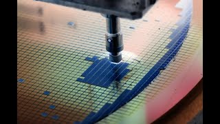
Common Etch Chemistries
Interactive Audio Lesson
Listen to a student-teacher conversation explaining the topic in a relatable way.
Introduction to Etch Chemistries
🔒 Unlock Audio Lesson
Sign up and enroll to listen to this audio lesson

Today we’re discussing common etch chemistries in semiconductor manufacturing. Can anyone tell me what they think an etching process involves?

Is it just about removing material from the wafer?
Exactly! Etching is used to remove specific materials to create defined patterns. Why do you think it’s important to select specific chemistries for different materials?

Because different materials have different properties? We have to avoid damage to other layers.
Correct! We need to maintain selectivity and precision in our etching processes. Let's explore some commonly used etch chemistries.
Common Etch Chemistries
🔒 Unlock Audio Lesson
Sign up and enroll to listen to this audio lesson

First, let's talk about SiO₂. What gases do you think we use to etch silicon dioxide?

I think it’s CF₄ or CHF₃?
Yes! CF₄ or CHF₃ are the typical choices. Can someone explain why these gases are used?

They probably provide the right mix of selectivity and etch profile?
Exactly! Now, what about silicon nitride? Anyone can tell me which gases are used there?
SF₆ or H₃PO₄ is used for Si₃N₄, right?
Correct! Each material needs a specific approach. Finally, aluminum uses Cl₂ or BCl₃ plasmas. Why do you think chlorine-based chemistries are used here?
Maybe they provide a good reaction at the right temperature?
Good guess! Chlorine effectively interacts with the aluminum to provide clean etching.
Applications and Implications of Etch Chemistries
🔒 Unlock Audio Lesson
Sign up and enroll to listen to this audio lesson
Let’s discuss how choosing the wrong etch chemistry could impact our manufacturing process. What do you think could happen?
It might damage the underlying layers or not etch properly.
Exactly! Poor selectivity can lead to defects in the circuit design. Can anyone think of how choosing the right gas is critical in achieving high precision?
Using the right gas increases the anisotropic etch profile, which is vital for smaller features!
Right! Understanding these properties enhances our ability to create intricate designs in semiconductor devices. This will lead us into our next topic about etching equipment.
Introduction & Overview
Read summaries of the section's main ideas at different levels of detail.
Quick Overview
Standard
In semiconductor fabrication, different common etch chemistries are employed to remove materials selectively. The section details specific chemicals used for etching various materials, highlighting the gases used for etching SiO₂, Si₃N₄, and aluminum, which are crucial for creating precise patterns in integrated circuits.
Detailed
Common Etch Chemistries
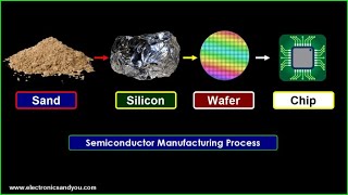
In the context of semiconductor manufacturing, etching processes utilize specific chemistries that are essential for patterning various materials on a silicon wafer. The section outlines the various chemicals that are commonly used to remove different materials:
- SiO₂ (Silicon Dioxide) is typically etched using CF₄ (carbon tetrafluoride) or CHF₃ (fluorinated hydrocarbons). These chemicals are effective in providing the desired selectivity and anisotropy necessary for modern semiconductor devices.
- Si₃N₄ (Silicon Nitride), another critical material in semiconductor multilayer structures, is usually etched away with SF₆ (sulfur hexafluoride) or H₃PO₄ (phosphoric acid). This demonstrates the need for different chemistries based on the material's properties and desired outcomes.
- Aluminum, a common conductor material in integrated circuits, requires the use of chlorine-based plasmas such as Cl₂ (chlorine) or BCl₃ (boron trichloride). These etch chemistries are vital for ensuring that aluminum layers can be selectively removed without adversely affecting other materials on the wafer.
Understanding these chemistries is paramount for semiconductor professionals as they define the operational parameters that impact etch selectivity, speed, and precision—all crucial for the successful fabrication of integrated circuits.
Youtube Videos


Audio Book
Dive deep into the subject with an immersive audiobook experience.
Etch Chemistries for SiO₂
Chapter 1 of 3
🔒 Unlock Audio Chapter
Sign up and enroll to access the full audio experience
Chapter Content
- SiO₂: Etched with CF₄ or CHF₃.
Detailed Explanation
This chunk discusses the specific chemistries used to etch silicon dioxide (SiO₂), a common material in semiconductor fabrication. The two chemical compounds mentioned, CF₄ (Carbon Tetrafluoride) and CHF₃ (Hydrofluorocarbon), are gases used in the etching process. When these gases are introduced into the etching equipment, they react with the SiO₂ material, effectively removing it from the surface of the wafer at controlled rates.
Examples & Analogies
Think of etching SiO₂ like using a specialized cleaner to remove a stain from a carpet. Just as different cleaners work on different types of stains, CF₄ and CHF₃ are designed to specifically react with SiO₂, ensuring effective removal without affecting the surrounding materials.
Etch Chemistries for Si₃N₄
Chapter 2 of 3
🔒 Unlock Audio Chapter
Sign up and enroll to access the full audio experience
Chapter Content
- Si₃N₄: Etched using SF₆ or H₃PO₄.
Detailed Explanation
In this chunk, we learn about the etching chemistries for silicon nitride (Si₃N₄). The etching processes utilize SF₆ (Sulfur Hexafluoride) and H₃PO₄ (Phosphoric Acid). SF₆ is a gas that, when ionized in the etcher's environment, can selectively react with Si₃N₄, whereas H₃PO₄ is typically used in a wet etching process. The choice between gas and liquid etchants allows for flexibility based on the precision and characteristics needed for the specific etching task.
Examples & Analogies
Imagine you have a delicate fabric that needs a specific stain removed. You might choose a special spray (SF₆) for targeted areas and a wash (H₃PO₄) for the overall cleaning process. Each method is chosen based on the fabric's properties, just like etchants are chosen based on the material being etched.
Etch Chemistries for Aluminum
Chapter 3 of 3
🔒 Unlock Audio Chapter
Sign up and enroll to access the full audio experience
Chapter Content
- Aluminum: Requires Cl₂ or BCl₃ plasmas.
Detailed Explanation
This chunk explains the etching chemistries for aluminum, a metallic layer commonly used in integrated circuits. The etching process utilizes chlorine gas (Cl₂) or boron trichloride (BCl₃) in plasma form. When these gases are ionized and directed toward the aluminum surface, they form reactive species that etch away the aluminum layer. This process is highly controlled to ensure that only the aluminum is removed without damaging the underlying layers.
Examples & Analogies
Consider this like using a highly corrosive acid to clean metal tools. Just as you’d ensure that only the rust is removed without harming the metal underneath, the etching process is honing in on the aluminum, leaving the other materials intact around it.
Key Concepts
-
Etching: A critical method in semiconductor processing to pattern materials.
-
Selectivity: Ensures unwanted materials are preserved while etching desired patterns.
-
Different gases: Varying chemistries are used for different materials such as SiO₂, Si₃N₄, and aluminum.
Examples & Applications
CF₄ or CHF₃ are used for etching SiO₂, demonstrating the importance of tailored chemistries.
Aluminum requires Cl₂ or BCl₃ for effective etching, highlighting the need for specific gas interactions.
Memory Aids
Interactive tools to help you remember key concepts
Rhymes
To etch SiO₂, CF₄’s the key, for Al use BCl₃, that’s the chemistry!
Stories
A semiconductor engineer named ‘Si’ often faced problems with etching gases. One day, he solved his issue by remembering CF₄ for SiO₂ and discovered BCl₃ was perfect for aluminum.
Memory Tools
Use 'CF' for 'Carbon Fluro' to remember CF₄ for SiO₂ etching!
Acronyms
Think of 'SAB' (Selectivity, Anisotropy, Balance) for remembering key properties during etching.
Flash Cards
Glossary
- Etching
A process to remove material from the surface of a substrate to form patterns.
- Selectivity
The ability to etch one material while preserving others underneath.
- Anisotropy
The directional dependence of a property, leading to vertical profiles during etching.
Reference links
Supplementary resources to enhance your learning experience.