
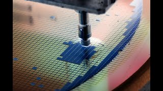
Step 4: Deposition Equipment
Interactive Audio Lesson
Listen to a student-teacher conversation explaining the topic in a relatable way.
PVD System
🔒 Unlock Audio Lesson
Sign up and enroll to listen to this audio lesson

Today, we’re going to learn about Physical Vapor Deposition, or PVD. Can anyone tell me what they think PVD involves?

Does it have something to do with depositing materials onto surfaces?
Exactly! PVD involves vaporizing material and then depositing it onto a substrate. It typically uses methods like sputtering, where argon ions target atoms to form thin films. Let’s remember PVD as a 'Perfect Vapor Delivery' system.

Why is that important in semiconductor manufacturing?
Great question! Thin films are critical for building layers like metals and dielectrics that are essential for devices.

What materials can be deposited using PVD?
Common materials include aluminum, titanium, and tungsten. Remember, ‘PVD = Perfect for Various Deposits’!
So to summarize, PVD is used for depositing thin films and is crucial for fabricating semiconductor devices by enabling precise material layers.
LPCVD and PECVD
🔒 Unlock Audio Lesson
Sign up and enroll to listen to this audio lesson

Now, let’s discuss Low-Pressure Chemical Vapor Deposition, or LPCVD, as well as Plasma-Enhanced Chemical Vapor Deposition, PECVD. Can someone start by explaining what these processes entail?

Do they both use gases to form films?
Correct! LPCVD typically operates at lower pressures to create uniform films and can coat complex geometries. On the other hand, PECVD uses plasma to enhance reactions at lower temperatures. That's particularly useful for sensitive materials.
What kind of applications do these have?
LPCVD is often used to deposit silicon nitride and oxide layers, while PECVD is great for low-k dielectrics. Here’s a mnemonic: ‘LPCVD for Layers, PECVD for Plasma!’
So, LPCVD would be better for high-temperature processes, I assume?
Not quite, LPCVD operates at low pressure but can still use higher temperatures. PECVD is our friend for low-temp applications! It's crucial to choose the right process based on the thermal budget.
In summary, LPCVD and PECVD are vital for materials that need specific deposition conditions due to their unique operational parameters.
ALD Chamber
🔒 Unlock Audio Lesson
Sign up and enroll to listen to this audio lesson
Finally, let’s delve into Atomic Layer Deposition, or ALD. Who can tell me how ALD differs from other deposition techniques?
I think it deposits one layer at a time, right?
Exactly! ALD is known for its layer-by-layer approach, allowing for atomic-level control of film thickness. Can anyone recall how a typical ALD cycle works?
Isn’t it something like exposing the surface to precursor A, then B, and purging in between?
That's correct! The cyclic process allows precise control over material deposition, vital for advanced transistors and capacitors.
What materials do we usually use with ALD?
Common ALD materials include high-k dielectrics and titanium nitride. Remember ALD as ‘Atomic Layer Delight’ for its precision!
To wrap up, ALD’s ability to deposit monolayers precisely makes it indispensable in the semiconductor field, especially for modern electronic devices.
Introduction & Overview
Read summaries of the section's main ideas at different levels of detail.
Quick Overview
Standard
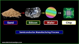
The section provides an overview of different deposition equipment such as PVD systems, LPCVD furnaces, PECVD reactors, and ALD chambers. Each type of equipment is discussed in terms of its operational principles and specific applications in the deposition process, focusing on their functionalities and advantages.
Detailed
Step 4: Deposition Equipment
This section delves into the various deposition equipment essential for semiconductor manufacturing, specifically highlighting their functions and operational principles. Understanding these devices is critical for successful implementation of deposition techniques such as Physical Vapor Deposition (PVD), Low-Pressure Chemical Vapor Deposition (LPCVD), Plasma-Enhanced Chemical Vapor Deposition (PECVD), and Atomic Layer Deposition (ALD).
Equipment Overview
- PVD System (Sputterer): Utilizes argon ions to target and deposit atoms onto substrates, delivering thin films necessary for various semiconductor layers.
- LPCVD Furnace: Designed for batch processing, ensuring conformal layer deposition, which is crucial for coatings on intricate geometries.
- PECVD Reactor: Operates at lower temperatures by stimulating the reactions with plasma, advantageous for sensitive materials.
- ALD Chamber: Enables precision at the angstrom level through a cycle of precursor exposures, with each cycle depositing a single monolayer of material, essential for high-k dielectrics and advanced node transistors.
The section emphasizes the significance of these devices in generating high-quality films crucial for integrated circuit functionality.
Youtube Videos


Audio Book
Dive deep into the subject with an immersive audiobook experience.
PVD System (Sputterer)
Chapter 1 of 5
🔒 Unlock Audio Chapter
Sign up and enroll to access the full audio experience
Chapter Content
- PVD System (Sputterer): Targets atoms using argon ions and deposits them.
Detailed Explanation
A Physical Vapor Deposition (PVD) system, particularly one using sputtering, works by directing argon ions at a target material. When the ions collide with the target, they dislodge atoms from its surface. The ejected atoms then travel through a vacuum environment to deposit onto a substrate, forming a thin film. This method is useful for creating layers of metals and other materials on surfaces like semiconductor wafers.
Examples & Analogies
Imagine the PVD process as shooting a paintball at a wall coated with paint. When the paintball (argon ion) hits the wall (target material), it splatters paint (target atoms) that can then land on a canvas (the substrate) to create a new layer of color. Just like layering paint gives the canvas a vibrant finish, deposition creates functional layers vital for semiconductor devices.
LPCVD Furnace
Chapter 2 of 5
🔒 Unlock Audio Chapter
Sign up and enroll to access the full audio experience
Chapter Content
- LPCVD Furnace: Batch processing for conformal layers.
Detailed Explanation
Low-Pressure Chemical Vapor Deposition (LPCVD) furnaces are used to deposit thin films in a batch process. In this setup, wafers are placed into the furnace, and gases react at lower pressures to form a solid layer on the wafers. This process allows for uniform layer deposition across multiple wafers at once, making it efficient for manufacturing. The conformality refers to the ability of the deposited layer to coat complex surface geometries evenly.
Examples & Analogies
Think of the LPCVD furnace as a large pizza oven where you can cook multiple pizzas at the same time. Instead of making each pizza one at a time (like traditional deposition), you bake them all in a batch. Just as the heat evenly cooks the toppings on each pizza, the LPCVD process ensures that the thin film is uniformly deposited across all wafers, even if they have some irregular shapes.
PECVD Reactor
Chapter 3 of 5
🔒 Unlock Audio Chapter
Sign up and enroll to access the full audio experience
Chapter Content
- PECVD Reactor: Low-temp films using plasma excitation.
Detailed Explanation
Plasma-Enhanced Chemical Vapor Deposition (PECVD) reactors allow for the deposition of thin films at lower temperatures compared to traditional CVD methods. This is especially beneficial for materials sensitive to heat. In PECVD, a plasma is created from the precursor gases, which facilitates the chemical reactions that produce the thin film layers on the substrates. The energy from the plasma helps to ensure the deposition of the materials even at lower temperatures, which can help protect delicate underlying structures.
Examples & Analogies
Picture making a delicate cake that might collapse if baked at high temperatures. Instead of using a conventional oven that requires high heat, you choose a microwave, which cooks the cake evenly without the risk of it falling apart. Similarly, PECVD utilizes plasma to deposit films at lower temperatures, ensuring that sensitive materials are not damaged during the process.
ALD Chamber
Chapter 4 of 5
🔒 Unlock Audio Chapter
Sign up and enroll to access the full audio experience
Chapter Content
- ALD Chamber: Angstrom-level thickness control.
Detailed Explanation
Atomic Layer Deposition (ALD) chambers are specialized environments designed for depositing thin films with atomic precision. The ALD process involves cycling through exposure to different gases that react on the surface in a self-limiting manner, allowing for extremely uniform layer growth. Each cycle results in the addition of a single atomic layer, enabling precise thickness control at the angstrom level.
Examples & Analogies
Think of the ALD process like adding a single layer of icing to a cake. Rather than slathering on a big glob of icing all at once, you carefully spread on just a tiny layer at a time, ensuring it is perfectly even and smooth before adding the next. Each cycle of ALD is like one of those careful icing applications, ensuring the final cake (or film) has the exact thickness and smoothness desired.
ALD Deposition Cycle
Chapter 5 of 5
🔒 Unlock Audio Chapter
Sign up and enroll to access the full audio experience
Chapter Content
- ALD Deposition Cycle:
- Precursor A exposure → Surface saturation
- Purge
- Precursor B exposure → Reaction with A
- Purge
Result: One monolayer deposited.
Detailed Explanation
The ALD deposition process involves a series of steps where chemicals are introduced to the substrate in controlled cycles. In the first step, a precursor gas A is introduced, saturating the surface. After reaching saturation, the chamber is purged to remove excess gas. Subsequently, precursor gas B is introduced, which reacts with A to form a solid layer. Finally, another purge clears any remaining gas, resulting in the addition of one atomic layer. This cyclic nature allows for extremely precise control over the resulting film thickness.
Examples & Analogies
Imagine you are stacking very delicate pieces of paper on top of each other to create a booklet. You carefully place one piece down, then take a moment to check for any overlaps before adding the next one. Each time you add a piece, you pause to ensure everything is in the right place before moving to the next layer. This is similar to the ALD cycle, where every step is carefully controlled to achieve the desired thickness, similar to stacking paper one sheet at a time.
Key Concepts
-
Key Concept 1: PVD allows for thin film deposition by vaporizing materials.
-
Key Concept 2: LPCVD operates under low pressure to create conformal layers.
-
Key Concept 3: PECVD uses plasma to enhance deposition processes at reduced temperatures.
-
Key Concept 4: ALD provides atomic-level control over thickness through cyclical deposition.
Examples & Applications
PVD is commonly used for depositing metal films such as aluminum in transistors.
LPCVD is often employed in the deposition of silicon nitride layers on complex geometries.
PECVD is favored for low-k dielectric materials in integrated circuits to improve performance.
ALD is used for depositing high-k materials essential for modern gate dielectrics.
Memory Aids
Interactive tools to help you remember key concepts
Rhymes
For films that are thin, PVD wins, layers crafted as the vapor spins.
Stories
Imagine a wizard who deposits gold dust layer by layer on a magic wand, carefully ensuring that each layer is just right—this is like ALD's careful process.
Memory Tools
Remember 'LPCVD for Low Pressure, PECVD for Plasma' to distinguish them easily.
Acronyms
PVD (Perfect Vapor Delivery), LPCVD (Low Pressure CVD) for Layers, PECVD (Plasma Energized CVD).
Flash Cards
Glossary
- PVD (Physical Vapor Deposition)
A deposition technique that involves vaporizing material and depositing it onto a substrate through processes such as sputtering.
- LPCVD (Low Pressure Chemical Vapor Deposition)
A technique for depositing thin films at lower pressures to ensure uniform coating and conformity on substrates.
- PECVD (Plasma Enhanced Chemical Vapor Deposition)
A method that uses plasma to enhance chemical reactions, allowing for deposition at lower temperatures.
- ALD (Atomic Layer Deposition)
A precise deposition technique that adds material one atomic layer at a time through a cyclical process of precursor exposure.
Reference links
Supplementary resources to enhance your learning experience.