
Introduction
Interactive Audio Lesson
Listen to a student-teacher conversation explaining the topic in a relatable way.
The Role of Deposition
🔒 Unlock Audio Lesson
Sign up and enroll to listen to this audio lesson

Let's start with deposition. This is a critical process where thin layers of material are deposited onto the wafer surface. Can anyone tell me why this is important for semiconductor devices?

I think it's important because it helps create the different layers required for transistors and other components?
Exactly! The deposition process is vital for layering materials such as gate oxides and metal contacts. To help you remember the key importance of deposition, think of 'D-Layers' — where 'D' stands for Deposition, and 'Layers' represents the multiple functional layers in devices.

Can you elaborate on different deposition techniques?
Certainly! We'll cover various techniques like Physical Vapor Deposition (PVD) and Chemical Vapor Deposition (CVD) later. For now, remember that the goal is to achieve a uniform layer for device functionality.

So if deposition is about applying layers, does that mean etching is about removing layers?
Spot on! And we'll discuss etching next. But before we move on, what do you think happens if there is an inconsistency in the deposition layer?

It could lead to defects or performance issues in the final product.
Exactly. Great job! Understanding the importance of these processes sets a strong foundation for our chapter.
The Function of Etching
🔒 Unlock Audio Lesson
Sign up and enroll to listen to this audio lesson

Now, let's shift gears to etching. Can anyone explain what etching does?
Etching removes material, right? To help create patterns?
Correct! Etching precisely removes materials to create the intricate patterns required for different electronic components. This process is defined during the lithography stage. So, remember 'E-Material Removal' for etching!
What types of etching are there?
There are mainly two: wet etching and dry etching. While wet etching uses liquid chemicals, dry etching employs gases in a vacuum. Can you see why dry etching might be preferred for certain applications?
Because it can be more precise and create more detailed structures?
Exactly! Precision is key. This insight into etching sets the stage for understanding how these processes intertwine in semiconductor manufacturing.
Introduction & Overview
Read summaries of the section's main ideas at different levels of detail.
Quick Overview
Standard
The introduction outlines how etching and deposition are essential processes that shape the multilayer structure of integrated circuits. It briefly highlights the role of deposition in forming thin material layers and the function of etching in selectively removing materials based on lithographic patterns.
Detailed
Introduction to Etching and Deposition in Semiconductor Manufacturing
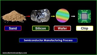
In semiconductor manufacturing, the processes of etching and deposition are pivotal for crafting the intricate multilayer structures found in integrated circuits.
Key Points Covered:
- Deposition: This involves the formation of thin layers of material on the wafer's surface, which is critical for building various layers that serve different functions in semiconductor devices.
- Etching: This process selectively removes materials to create patterns defined during the lithography stage, allowing for precise structuring of the circuits.
What This Chapter Includes:
- A comprehensive exploration of various etching mechanisms, classifications, and the equipment used.
- A discussion on common deposition techniques essential for constructing conductive, insulating, and barrier layers in microelectronics.
Youtube Videos


Audio Book
Dive deep into the subject with an immersive audiobook experience.
Importance of Etching and Deposition in Semiconductor Manufacturing
Chapter 1 of 4
🔒 Unlock Audio Chapter
Sign up and enroll to access the full audio experience
Chapter Content
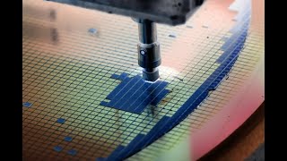
In semiconductor manufacturing, etching and deposition are two essential processes that form and sculpt the multilayer structure of an integrated circuit.
Detailed Explanation
Etching and deposition are crucial steps in creating integrated circuits, which are the building blocks of modern electronic devices. Etching is the process of removing specific materials from the surface of a semiconductor wafer, whereas deposition involves adding new materials to build up layers. These processes work together to create the complex structures needed in integrated circuits.
Examples & Analogies
Think of integrated circuits like a cake with layers - deposition is like adding layers of frosting (new materials), and etching is like cutting sections out of those layers to create designs (removing materials). Together, they help create the final look and functionality of the cake.
Deposition Process Overview
Chapter 2 of 4
🔒 Unlock Audio Chapter
Sign up and enroll to access the full audio experience
Chapter Content
Deposition involves forming thin layers of material on the wafer surface.
Detailed Explanation
During the deposition process, a thin layer of material is applied to the surface of the wafer to create various functional components of the circuit. This layer can be made from different types of materials depending on the application and requirements, such as metals for electrical connections or insulators for separating different circuit elements.
Examples & Analogies
Imagine painting a wall in your home. Just as you carefully apply paint to create an even coat and achieve the desired color and finish, in semiconductor manufacturing, deposition is about carefully layering materials to ensure each part of the circuit functions perfectly.
Etching Process Overview
Chapter 3 of 4
🔒 Unlock Audio Chapter
Sign up and enroll to access the full audio experience
Chapter Content
Etching selectively removes materials to create patterns defined by the lithography stage.
Detailed Explanation
In the etching process, predefined patterns are created on the wafer by selectively removing certain materials. This is done after a layer of photoresist has been applied and exposed to light, which defines the areas that will remain and those that will be etched away. The result is a specific pattern that is critical for the functioning of the integrated circuit.
Examples & Analogies
If you've ever used a stencil to spray paint a design on a surface, you've used a method similar to etching. The areas not covered by the stencil remain untouched, while the exposed areas are painted (removed), creating the desired design.
Overview of the Chapter
Chapter 4 of 4
🔒 Unlock Audio Chapter
Sign up and enroll to access the full audio experience
Chapter Content
This chapter provides:
● A detailed exploration of etching mechanisms, classifications, and equipment.
● Common deposition techniques used to build conductive, insulating, and barrier layers.
Detailed Explanation
The chapter will delve deeper into the specifics of both etching and deposition processes. It will cover different types of etching mechanisms and classify them according to their nature, as well as introduce the equipment used in these processes. Additionally, the various techniques for deposition required for constructing the layers will be discussed, including those for conductive, insulating, and barrier layers.
Examples & Analogies
Consider building a skyscraper – first, you need a solid foundation (deposition of layers), then you need to carve out windows and doors (etching). Just like construction involves multiple steps and techniques to ensure a stable and functional building, semiconductor fabrication is complex and requires specialized knowledge and tools.
Key Concepts
-
Deposition: The process of applying layers of material on semiconductor wafers.
-
Etching: The selective removal of material to form patterns.
-
Lithography: A critical step that defines how patterns will be etched into the material.
Examples & Applications
In semiconductor manufacturing, deposition techniques like PVD and CVD are utilized for various applications, such as depositing silicon dioxide and metal layers.
Etching techniques are employed to create precise patterns in semiconductor devices, for example, making contact holes for interconnects.
Memory Aids
Interactive tools to help you remember key concepts
Rhymes
Etch it, sketch it, on the wafer's plot, deposit the layers, that’s how we begin the lot!
Stories
Imagine an artist layer by layer painting on a canvas, and then using a chisel to carve specific patterns into their masterpiece; this is akin to how deposition and etching operate in semiconductor manufacturing.
Memory Tools
D-E for Data Entry, where 'D' represents Deposition and 'E' represents Etching – think of them as processes that add and subtract materials.
Acronyms
P-L for Process Layers, where 'P' stands for the layering process of Deposition and 'L' stands for the patterning process of Etching.
Flash Cards
Glossary
- Deposition
The process of depositing thin layers of material onto a substrate.
- Etching
A process that removes material to create specific patterns on a substrate.
- Lithography
A technique used to transfer patterns onto a surface.
Reference links
Supplementary resources to enhance your learning experience.