
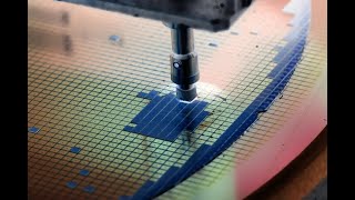
Step 3: Deposition Processes
Interactive Audio Lesson
Listen to a student-teacher conversation explaining the topic in a relatable way.
Overview of Deposition Processes
🔒 Unlock Audio Lesson
Sign up and enroll to listen to this audio lesson

Welcome class! Today, we'll explore deposition processes in semiconductor manufacturing, which are crucial for building layers on wafers. Can anyone tell me what deposition means?

I think it’s about adding materials to the wafer.
That's right! Deposition involves adding thin layers of materials to semiconductor devices. There are several techniques, like PVD and CVD. Let’s start with why deposition matters.

Is it just for making transistors?
Great question! It’s not just for transistors. We also use deposition for interconnects and isolation layers. Remember; we can use the acronym TIC: Transistors, Interconnects, and Coatings!
Understanding PVD and CVD
🔒 Unlock Audio Lesson
Sign up and enroll to listen to this audio lesson

Let's look at PVD first. Who can explain how it works?

It vaporizes materials and deposits them on the wafer in a vacuum, right?
Exactly! PVD is commonly used for metals like Aluminum and Titanium. What do you think the challenges of using PVD might be?

Maybe controlling the thickness?
Correct! Thickness uniformity is critical. Now, how about CVD? Anyone knows its key feature?
CVD uses gases to form a solid layer on the wafer.
Exactly! CVD is useful for materials like SiO₂ and SiN. Let’s remember it with the acronym GASF: Gases React at the Surface Forming a layer.
Advanced Deposition Techniques: PECVD and ALD
🔒 Unlock Audio Lesson
Sign up and enroll to listen to this audio lesson
Next, let’s cover PECVD and ALD. How are they different from PVD and CVD?
PECVD uses plasma at lower temperatures?
Correct! PECVD is excellent for low-k dielectrics. Now, can anyone explain ALD?
ALD deposits material atom by atom, right?
Yes! It’s known for its atomic-level precision, making it ideal for advanced nodes. Remember the mnemonic ALD: Accurate Layer Deposition!
Applications in Semiconductor Manufacturing
🔒 Unlock Audio Lesson
Sign up and enroll to listen to this audio lesson
To wrap up, let’s discuss application areas of these techniques. How does deposition affect transistors and circuits?
It affects how they conduct electricity and how small they can be made!
Exactly! The choice of deposition technique impacts device performance. Remember the phrase 'Fit for Purpose.' It's crucial to choose the right technique based on material and function.
And that impacts the overall device efficiency?
Spot on! The selection of deposition processes ensures the functionalities like conductivity and insulation are optimized.
Introduction & Overview
Read summaries of the section's main ideas at different levels of detail.
Quick Overview
Standard
In semiconductor manufacturing, deposition processes play a pivotal role in layering materials essential for transistors, interconnects, and isolation. Different techniques like Physical Vapor Deposition and Chemical Vapor Deposition are used to create these layers, impacting the performance and efficiency of electronic devices.
Detailed
Detailed Summary of Deposition Processes
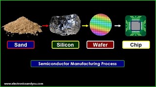
In semiconductor fabrication, deposition processes are indispensable for creating the functional layers necessary for components such as transistors, interconnects, and dielectric barriers. The section outlines four primary deposition techniques:
- Physical Vapor Deposition (PVD): Involves vaporizing a material in a vacuum and depositing it onto the wafer. Common materials include Aluminum (Al), Titanium (Ti), and Tungsten (W).
- Chemical Vapor Deposition (CVD): Utilizes reactive gases to form a film on the wafer surface, typically consisting of materials like Silicon Dioxide (SiO₂), Silicon Nitride (SiN), and polysilicon.
- Plasma-Enhanced CVD (PECVD): Operates at lower temperatures using plasma, ideal for low-k dielectrics.
- Atomic Layer Deposition (ALD): Features self-limiting chemical reactions to deposit materials layer-by-layer with atomic precision, important for high-k oxides and materials like Titanium Nitride (TiN).
- Spin Coating: Primarily used for applying photoresist or polymer layers.
These techniques are critically evaluated for their applications in transistor technology and circuit integration, emphasizing the importance of material compatibility, feature size, and temperature tolerance. Understanding these processes is pivotal for advancing semiconductor technology and enhancing device performance.
Youtube Videos


Audio Book
Dive deep into the subject with an immersive audiobook experience.
Purpose of Deposition Processes
Chapter 1 of 2
🔒 Unlock Audio Chapter
Sign up and enroll to access the full audio experience
Chapter Content
Deposition builds functional layers required for:
● Transistors (gate oxide, metal contacts)
● Interconnects (metal layers)
● Isolation (dielectric barriers)
Detailed Explanation
Deposition processes are essential in semiconductor manufacturing because they create the functional layers that make up various components of electronic devices. Each type of layer has a specific role:
- Transistors require gate oxides for insulation and metal contacts for connecting to other parts of the circuit.
- Interconnects consist of metal layers that facilitate electrical connections among transistors and other components.
- Isolation layers, also called dielectric barriers, are used to prevent unwanted electrical interactions between different components, ensuring the circuit functions correctly.
Examples & Analogies
Think of deposition processes like building a sandwich. Each layer of the sandwich (like bread, lettuce, tomato, and meat) represents a different functional layer in a semiconductor. Just as each ingredient adds to the overall flavor and structure of the sandwich, each deposited layer contributes to the performance and functionality of the electronic device.
Main Deposition Techniques Overview
Chapter 2 of 2
🔒 Unlock Audio Chapter
Sign up and enroll to access the full audio experience
Chapter Content
• Main Deposition Techniques:
Technique Description Typical Materials
Physical Vapor Deposition Material vaporized in vacuum and Al, Ti, W
(PVD) deposited
Chemical Vapor Gases react on wafer to form a film SiO₂, SiN, polysilicon
Deposition (CVD)
Plasma-Enhanced CVD CVD at lower temperature using Low-k dielectrics
(PECVD) plasma
Atomic Layer Deposition Self-limiting chemical reactions High-k oxides, TiN
(ALD) layer-by-layer
Spin Coating Used mainly for photoresist or Resist, planarization
polymer deposition layers
Detailed Explanation
There are several techniques for depositing materials in semiconductor fabrication, each serving different functions and using various materials:
1. Physical Vapor Deposition (PVD): In this method, materials are vaporized in a vacuum and then deposited onto the wafer. Common materials include aluminum, titanium, and tungsten. This technique is beneficial for creating thick metal layers.
2. Chemical Vapor Deposition (CVD): CVD employs gases that react chemically on the surface of the wafer to form a solid film. It is commonly used for materials like silicon dioxide (SiO₂) and silicon nitride (SiN).
3. Plasma-Enhanced CVD (PECVD): This method uses plasma to enhance the CVD process, allowing films to be formed at lower temperatures. It is particularly useful for low-permittivity dielectrics, which help reduce capacitance in electronic devices.
4. Atomic Layer Deposition (ALD): In ALD, materials are deposited in a layer-by-layer fashion through self-limiting chemical reactions. This technique is ideal for high-k dielectrics and TiN, offering precise control over thickness at the atomic level.
5. Spin Coating: This technique is primarily used for applying photoresist or polymer layers to the wafer by spinning it at high speeds, which spreads the material evenly over the surface.
Examples & Analogies
Consider the different deposition techniques as different cooking methods. PVD is like grilling, where you apply heat and wait for the meat to form a crust. CVD is similar to baking, where you have ingredients that react to create something new. PECVD can be viewed as a slow cooker, allowing for gentle preparation at lower temperatures. ALD resembles a meticulous layer of lasagna, where each layer is added one at a time with precise timing. Lastly, spin coating is like frosting a cake—spreading a smooth layer over the surface evenly.
Key Concepts
-
PVD: A method of depositing materials in a vacuum.
-
CVD: Uses gas-phase chemical reactions to deposit materials.
-
PECVD: A variant of CVD that operates with plasma for enhanced reactions.
-
ALD: Precise layer-by-layer deposition technique.
-
Spin Coating: Technique for applying thin layers of liquid materials.
Examples & Applications
Using PVD to deposit Aluminum contacts on a silicon wafer for transistor fabrication.
Employing CVD to create a silicon dioxide layer for dielectric isolation in integrated circuits.
Implementing PECVD to deposit low-k dielectric films for reducing capacitance in high-speed circuits.
Utilizing ALD for depositing high-k gate dielectrics in advanced technology nodes.
Memory Aids
Interactive tools to help you remember key concepts
Rhymes
PVD, high and dry, in a vacuum it goes to sky. CVD comes with a gas, creating layers that are top class!
Stories
Imagine a wafer named 'Wavy'. Wavy wishes to dress with layers. First, PVD gives it shiny suits made of metal, followed by CVD wrapping it in insulating gases!
Memory Tools
Remember 'P-C-A-S': PVD - Chemical Vapor - Atomic Layer - Spin to recall the main deposition processes.
Acronyms
Use the acronym TIC to remember
for Transistors
for Interconnects
for Coatings
important layers in semiconductor tech!
Flash Cards
Glossary
- Physical Vapor Deposition (PVD)
A vacuum deposition method where material is vaporized and then condensed onto the substrate.
- Chemical Vapor Deposition (CVD)
A process that uses chemical reactions of gaseous precursors to form a solid material film on a substrate.
- PlasmaEnhanced CVD (PECVD)
CVD that uses plasma to enhance the chemical reaction rates at lower temperatures.
- Atomic Layer Deposition (ALD)
A thin-film deposition technique that deposits material layer-by-layer using self-limiting chemical reactions.
- Spin Coating
A technique used to apply uniform thin layers of liquid materials onto a substrate by spinning it.
Reference links
Supplementary resources to enhance your learning experience.