
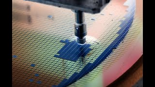
Etching and Deposition Processes
Interactive Audio Lesson
Listen to a student-teacher conversation explaining the topic in a relatable way.
Introduction to Etching and Deposition
🔒 Unlock Audio Lesson
Sign up and enroll to listen to this audio lesson

Today, we will explore the processes of etching and deposition, which are essential in creating integrated circuits. Can anyone tell me what deposition means?

Isn’t it about putting down layers of materials on the wafer?
Exactly! Deposition refers to the process where we form thin layers on the wafer surface. And how about etching?

I think it means removing certain materials?
Yes! Etching selectively removes materials based on the patterns defined by lithography. Remember, we can think of deposition as 'layering up' and etching as 'carving out'!

Can you explain why both are important?
Sure! They are crucial for creating complex structures in semiconductors. Without etching, we don’t get patterns, and without deposition, we wouldn't have the necessary materials for function. It's a balance!

Got it! So they work together to make functional devices?
Exactly! Let's move on to the challenges we face when working at the nanoscale.
Etching Processes
🔒 Unlock Audio Lesson
Sign up and enroll to listen to this audio lesson

Now let's look closely at the types of etching. What can you tell me about wet etching?
Wet etching uses liquid chemicals, right?
Correct! It’s simpler but tends to be isotropic. What does isotropic mean in this context?
It means the etching happens equally in all directions?
Exactly! And how does dry etching differ?
I think dry etching uses gases and is more precise because it’s anisotropic?
Good! Dry etching is indeed used for high-resolution patterns. What about reactive ion etching?
I remember it's a combination of plasma and ion bombardment!
Correct! This method is vital for advanced nodes. Remember 'WET and DRY - the etching world’s two guys!' to help you recall these types.
Deposition Techniques
🔒 Unlock Audio Lesson
Sign up and enroll to listen to this audio lesson
Let's shift gears and discuss deposition processes. Who can describe what Physical Vapor Deposition (PVD) is?
PVD vaporizes a material in a vacuum, right?
Yes! And what kind of materials do we commonly use with PVD?
Aluminum and titanium, if I remember correctly?
Exactly! Now, what about Chemical Vapor Deposition (CVD)?
CVD uses gases that react on the wafer to create a solid film.
Spot on! And can anyone explain what PECVD is?
It’s CVD but enhanced by plasma at lower temperatures!
Fantastic! Just remember PEM when you think of PECVD: Plasma, Enhanced, and Material creation!
Challenges in Etching and Deposition
🔒 Unlock Audio Lesson
Sign up and enroll to listen to this audio lesson
Now, let’s discuss some of the challenges we encounter in these processes. What do you think is the main issue when depositing materials at nanoscale?
Achieving uniformity over complex shapes is tough!
Very true! And what about etching? What are some specific challenges?
We need high precision and selectivity, and depth control is vital.
Exactly! We want to minimize damage while ensuring good vertical profiles. That’s why we must understand our materials and techniques well.
So, it’s about striking a balance and being selective?
Perfectly put! Remember the mnemonic: 'Precision, Selectivity, and Damage control are our goals!'
Equipment Overview
🔒 Unlock Audio Lesson
Sign up and enroll to listen to this audio lesson
Finally, let’s review the equipment! What equipment do we use for dry etching?
We would use a Reactive Ion Etching system.
Correct! And what about wet etching?
That would be the wet bench, right?
Yes! Now for deposition, what about a PVD system?
It's used for sputtering and target atoms!
Excellent! Remember also the ALD chamber for atomic-level control of thickness. You could think of it as A for 'Atomic', L for 'Layering', and D for 'Depositing'.
Introduction & Overview
Read summaries of the section's main ideas at different levels of detail.
Quick Overview
Standard
This section delves into etching and deposition processes, focusing on their definitions, challenges, mechanisms, techniques, and equipment involved in semiconductor manufacturing. It highlights the importance of achieving precision in nanoscale applications.
Detailed
Etching and Deposition Processes
In semiconductor manufacturing, two of the foundational processes are etching and deposition. These processes enable the fabrication of multilayer structures that are crucial to integrated circuits. In simple terms, deposition refers to the application of thin layers of materials on the wafer surface, while etching selectively removes materials based on designs created during lithography.
The section addresses the specific challenges faced when trying to scale down devices to nanoscale dimensions, such as achieving uniform material deposition over complex shapes and conducting etching with high precision and selectivity.
Etching Processes
Various types of etching methods are explored:
- Wet Etching: Utilizes liquid chemical etchants for isotropic material removal.
- Dry Etching: Employs plasma or gases in a vacuum to achieve anisotropic etching, vital for detailed patterns.
- Reactive Ion Etching (RIE): A more advanced form that results in precise etching by combining both plasma and directional ion bombardment.
Key etching properties include selectivity, which allows for the removal of specific materials without impacting others, and etch rate control, critical for ensuring accuracy in dimensions.
Deposition Processes
Deposition processes create functional layers required for transistors, interconnects, and insulation. Various techniques include:
- Physical Vapor Deposition (PVD): Involves vaporization of materials in a vacuum.
- Chemical Vapor Deposition (CVD): Involves chemical reactions of gases on wafer surfaces to form films.
- Plasma-Enhanced CVD (PECVD): Implements plasma for low-temperature film production.
- Atomic Layer Deposition (ALD): Allows for precise control with layer-by-layer deposition.
- Spin Coating: Widely used for applying photoresist.
Equipment
The section also emphasizes equipment like RIE systems for dry etching, wet benches for wet etching, and various deposition systems that utilize different techniques to achieve desired properties in layers. Through a combination of these processes, microelectronic devices are fabricated to meet the rigorous standards of performance and reliability required today.
In conclusion, etching and deposition processes are pivotal in the continuous advancement of semiconductor technology, leading to the implementation of increasingly complex and efficient device designs.
Youtube Videos


Audio Book
Dive deep into the subject with an immersive audiobook experience.
Introduction to Etching and Deposition
Chapter 1 of 4
🔒 Unlock Audio Chapter
Sign up and enroll to access the full audio experience
Chapter Content
In semiconductor manufacturing, etching and deposition are two essential processes that form and sculpt the multilayer structure of an integrated circuit.
- Deposition involves forming thin layers of material on the wafer surface.
- Etching selectively removes materials to create patterns defined by the lithography stage.
This chapter provides:
- A detailed exploration of etching mechanisms, classifications, and equipment.
- Common deposition techniques used to build conductive, insulating, and barrier layers.
Detailed Explanation
This section introduces the critical processes of etching and deposition in semiconductor manufacturing. It explains that deposition is the method of creating thin films of material on a semiconductor wafer, which is foundational for constructing various electronic components. In contrast, etching is the process that carves out specific patterns on the wafer by selectively removing material, a task that is guided by earlier lithography steps. This introduction sets the stage for detailed discussions about how these processes operate and are categorized.
Examples & Analogies
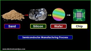
Think of semiconductor manufacturing like building a multi-layer cake. Deposition is like adding layers of frosting on the cake, ensuring that each layer is smooth and uniform. Etching, on the other hand, is like carving out shapes in the frosting to create decorations. Both processes are vital for the final look and function of the cake!
Challenges in Etching and Deposition
Chapter 2 of 4
🔒 Unlock Audio Chapter
Sign up and enroll to access the full audio experience
Chapter Content
To realize nanoscale devices:
- Materials must be deposited uniformly over complex topographies.
- Etching must occur with atomic-scale precision, anisotropy, and selectivity.
The main challenge lies in achieving accurate vertical profiles, minimizing damage, and enabling high aspect-ratio patterning in multi-layer stacks.
Detailed Explanation
This chunk outlines the significant challenges that engineers face when working with nanoscale devices. Depositing material uniformly becomes complex when the surface features are not flat but instead have various elevations and contours. Etching needs to be incredibly precise at an atomic level, which means that the processes must be controlled very carefully to ensure that only the desired material is removed while maintaining the integrity of the underlying layers. Furthermore, managing vertical profiles and minimizing damage during these processes is crucial, particularly when dealing with multiple stacked layers.
Examples & Analogies
Imagine trying to lay a smooth, even layer of paint on a textured wall. If your surface is uneven, the paint can end up pooling in some areas while not covering others adequately. Similarly, in semiconductor manufacturing, if deposition isn't uniform over a complex surface, it can lead to defects or improperly functioning devices.
Types of Etching
Chapter 3 of 4
🔒 Unlock Audio Chapter
Sign up and enroll to access the full audio experience
Chapter Content
• Types of Etching:
Type Description Use Case
Wet Etching Chemical etchants dissolve materials in liquid phase. Simpler, but isotropic
Dry Etching Uses plasma or gases in vacuum to remove material. Anisotropic, high-resolution
Reactive Ion Etching (RIE) Combines plasma and directional ion bombardment. Precise, used in advanced nodes
• Key Properties of Etching:
- Selectivity: Ability to remove one material without affecting others.
- Anisotropy: Directional etching, important for vertical profiles.
- Etch Rate Control: Vital for critical dimension accuracy.
Detailed Explanation
This chunk details the different types of etching processes along with their characteristics and applications. Wet etching is a simpler method using liquid chemicals to dissolve materials, but it often results in isotropic patterns (where etching occurs equally in all directions). Dry etching, on the other hand, utilizes gases or plasmas within a vacuum to create more precise, anisotropic etching that is essential for creating defined vertical profiles. Reactive Ion Etching (RIE) is a specialized technique that enhances the precision further by using energetic ions. The properties of selectivity, anisotropy, and etch rate control are crucial for achieving the desired results without causing unwanted damage.
Examples & Analogies
Consider different ways of sculpting a statue. Using a chisel (dry etching) allows for precise cuts and detailed work compared to using just a hammer (wet etching), which might distribute force too broadly and affect other areas. In essence, the choice of tools (etching methods) determines the quality of the final sculpture (semiconductor features).
Common Etch Chemistries
Chapter 4 of 4
🔒 Unlock Audio Chapter
Sign up and enroll to access the full audio experience
Chapter Content
• Common Etch Chemistries:
- SiO₂: Etched with CF₄ or CHF₃.
- Si₃N₄: Etched using SF₆ or H₃PO₄.
- Aluminum: Requires Cl₂ or BCl₃ plasmas.
Detailed Explanation
This section provides specifics about the chemicals used in etching different materials. For instance, SiO₂ is often etched using gases like CF₄ or CHF₃, while Si₃N₄ utilizes SF₆ or H₃PO₄. Each material requires a specific chemistry to effectively remove it without affecting the underlying layers. The selection of etching agents is crucial for optimizing the etching process and ensuring the desired outcome.
Examples & Analogies
Think of etching materials like cooking ingredients in a dish. Just like you need the right spices and flavors to extract the best taste from ingredients, choosing the appropriate chemicals for etching is essential to achieve the best results on the semiconductor wafer.
Key Concepts
-
Etching: A critical process for removing material to create circuit patterns.
-
Deposition: The addition of thin films required for integrated circuit functionality.
-
Selectivity: The ability to specifically remove or leave materials intact during processing.
-
Anisotropy: A quality of etching in which removal is directionally controlled, crucial for achieving depth during etching.
Examples & Applications
An example of etching is using RIE to create high-resolution patterns for transistors in advanced microchips.
ALD can be exemplified by the careful creation of high-k gate dielectrics, vital for modern transistor performance.
Memory Aids
Interactive tools to help you remember key concepts
Rhymes
Etch and Deposition, a fabrication dance, both working together to enhance.
Stories
Once there was a chef (deposition) who layered tasty pies, and a sculptor (etching) who carefully carved them out. Together, they created stunning desserts!
Memory Tools
For etching, remember 'SAD' - Selective, Anisotropic, Depth control.
Acronyms
LEAD for deposition techniques
Layering
Enhancing
Applying
Depositing.
Flash Cards
Glossary
- Deposition
The process of adding layers of material onto the surface of a wafer.
- Etching
The method for selectively removing material to create patterns on the wafer.
- Selectivity
The ability to remove one material without affecting others.
- Anisotropy
The directional dependence of etching, important for achieving vertical profiles.
- Physical Vapor Deposition (PVD)
A process that vaporizes materials in a vacuum and deposits them onto a substrate.
- Chemical Vapor Deposition (CVD)
A process that uses chemical reactions of gases to form thin films on a substrate.
- PlasmaEnhanced CVD (PECVD)
A variant of CVD that employs plasma to enable lower-temperature processing.
- Reactive Ion Etching (RIE)
A dry etching method that combines plasma and ion bombardment for precision.
- Atomic Layer Deposition (ALD)
A technique for depositing thin films one atomic layer at a time.
Reference links
Supplementary resources to enhance your learning experience.