
Problem Statement
Interactive Audio Lesson
Listen to a student-teacher conversation explaining the topic in a relatable way.
Importance of Uniform Deposition
🔒 Unlock Audio Lesson
Sign up and enroll to listen to this audio lesson

Today, we will begin our discussion on the problem statement by talking about uniform deposition. Why do we need materials to be deposited uniformly on complex surfaces?

I think it’s important to ensure that all parts of the device work well together.
Exactly! Uniform deposition allows for consistent electrical properties across the device. This is crucial as variations can lead to failures. Can anyone think of a real-world analogy to illustrate this?

Like how a thick coat of paint on some parts of a wall can lead to uneven colors or textures?
Good analogy! Just as uneven paint affects the wall's appearance, non-uniform deposition affects a semiconductor’s functionality. Let’s remember the acronym ‘P.O.W.E.R.’ for 'Precision, Optimality, With Efficiency and Reliability' to keep this in mind.

So if we don’t have precision, we won’t have reliability in devices?
Precisely! Now, let’s summarize: Uniform deposition is vital for consistent device performance and reliability. Any questions?
Challenges in Etching Precision
🔒 Unlock Audio Lesson
Sign up and enroll to listen to this audio lesson

Now, let’s transition to etching. One of the main requirements for effective etching is precision. Why do you think precision is so critical in this process?

It probably affects how accurately we can shape the features on the wafer.
Exactly! Precision ensures that we can create specific patterns without affecting other materials. This concept of anisotropy in etching must be taken seriously. Can someone give me an example of how this might look?
I guess it’s like carving a sculpture where you want certain features to be sharp and well-defined without damaging the surrounding areas?
Great example! That’s the essence of etching in semiconductor manufacturing. Remember the mnemonic ‘A.C.E.’ for ‘Anisotropic Control for Etching’ — it summarizes what you need to focus on when etching.
So good control will mean better features?
Absolutely. Precision is key! So to recap, precision and control in etching define the success of creating patterns in semiconductors. Any further questions?
Managing Damage and Aspect Ratios
🔒 Unlock Audio Lesson
Sign up and enroll to listen to this audio lesson
Finally, let's discuss minimizing damage and achieving high aspect ratios. Why are these factors important?
If there’s too much damage, it could ruin the device's performance down the line?
Correct! Damage can degrade performance or lead to failure. Now, can anyone explain why high aspect ratios are desired?
It seems like it allows for more compact designs, which are important as devices get smaller?
Exactly! Compactness and efficiency are key. Let’s finalize our session with a memory aid: ‘D.A.R.E.’ which stands for ‘Damage Avoidance and Ratio Efficiency.’ Remember this when thinking about our challenges: minimization of damage and achieving the desired aspect ratios are crucial for success!
So, if we focus on D.A.R.E., we can optimize both performance and design?
Exactly! Great participation today! To summarize: Managing damage and achieving high aspect ratios are essential for modern semiconductor devices. Great strides have been made, but there's always more to learn!
Introduction & Overview
Read summaries of the section's main ideas at different levels of detail.
Quick Overview
Standard
In this section, the main challenges of creating nanoscale devices are discussed, focusing on the need for uniform material deposition over complex surfaces, atomic-scale etching precision, and the importance of achieving accurate vertical profiles and minimizing damage during the fabrication processes.
Detailed
Problem Statement
In the realm of semiconductor manufacturing, the realization of nanoscale devices presents significant challenges that must be meticulously addressed. This section highlights the key issues surrounding two critical fabrication processes: deposition and etching. The complexity of current semiconductor devices necessitates that:
- Uniform Deposition: Materials must be deposited uniformly across intricate topographies to ensure functionality and reliability across all device components.
- Precision in Etching: The etching process needs to achieve atomic-scale precision, maintaining selectivity and directional (anisotropic) properties to produce intricate patterns that define the device architecture.
The core challenges tied to these processes include:
- Accurate Vertical Profiles: It’s crucial to enable precise control over vertical profiles within multilayer stacks to ensure effective device performance.
- Minimizing Damage: Efforts must be made to reduce any potential damage incurred during these processes, as this can adversely impact device efficacy.
- High Aspect-Ratio Patterning: Achieving high aspect ratios in feature design is essential for enhancing the capabilities of modern semiconductor devices.
These factors underscore the intricate balance of precision, reliability, and performance that must be maintained in semiconductor fabrication.
Youtube Videos


Audio Book
Dive deep into the subject with an immersive audiobook experience.
Uniform Material Deposition
Chapter 1 of 3
🔒 Unlock Audio Chapter
Sign up and enroll to access the full audio experience
Chapter Content
To realize nanoscale devices:
- Materials must be deposited uniformly over complex topographies.
Detailed Explanation
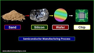
In the manufacturing of nanoscale devices, one critical requirement is that the materials are deposited uniformly. This means that when layers of materials are applied to the surface of the semiconductor wafer, they should cover every part of its surface evenly, even if that surface has intricate features or varying heights. If the deposition is uneven, it can lead to issues in the performance of the device as the functionalities depend on the consistency of the material layers.
Examples & Analogies
Think of spreading icing on a cake. If you apply the icing uniformly, each bite of the cake will have the same sweetness. However, if you apply it unevenly, some bites will be too sweet (too much icing) while others will be bland (not enough icing). This analogy illustrates the importance of uniformity in semiconductor material deposition.
Precision of Etching
Chapter 2 of 3
🔒 Unlock Audio Chapter
Sign up and enroll to access the full audio experience
Chapter Content
Etching must occur with atomic-scale precision, anisotropy, and selectivity.
Detailed Explanation
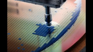
Etching is a process used to remove material from the wafer to achieve specific designs. For modern semiconductor devices, etching needs to be exceptionally precise, down to the atomic scale. Anisotropy refers to the directional nature of the etching process, where etching should primarily occur in a vertical manner to maintain the intended design's accuracy. Selectivity means the etching process should remove one material without affecting others, which is crucial for maintaining the integrity of different layers on the chip.
Examples & Analogies
Imagine you are sculpting a statue from a block of marble. If you carefully chip away at the marble from the top without affecting the underlying parts, you can create finely detailed features. If you were to chip away indiscriminately, the statue might end up losing its shape, just like selective etching preserves essential materials while removing others.
Challenges in Etching
Chapter 3 of 3
🔒 Unlock Audio Chapter
Sign up and enroll to access the full audio experience
Chapter Content
The main challenge lies in achieving accurate vertical profiles, minimizing damage, and enabling high aspect-ratio patterning in multi-layer stacks.
Detailed Explanation
In the context of etching, one of the significant challenges encountered is achieving accurate vertical profiles of the etched features. This means that the walls of the etched structures should be straight and not slanted. Additionally, minimizing damage to the substrate or other layers during the etching process is essential, as any unintended damage can affect the device's functionality. High aspect-ratio patterning means creating features that are much taller than they are wide, which is increasingly important for complex integrated circuits that require advanced designs.
Examples & Analogies
Consider building a tall skyscraper. The columns need to be straight (accurate vertical profiles), and any damage to the foundational structure can result in serious issues for the entire building. The height of the building compared to its base represents high aspect-ratio patterning, emphasizing the need for precision in the construction process to stand tall.
Key Concepts
-
Uniform Deposition: Essential for reliable device functionality, ensuring consistent performance across all areas of the semiconductor.
-
Etching Precision: Critical for creating fine patterns, requiring directionality (anisotropy) and selectivity in the removal of material.
-
High Aspect Ratios: Important for compact device designs, promoting efficiency in semiconductor architecture.
-
Damage Management: Reducing damage during etching and deposition can preserve device performance and longevity.
Examples & Applications
In semiconductor devices, the consistent deposition of silicon dioxide over a substrate ensures effective insulation and prevents electrical leakage.
When etching patterns for transistors, achieving high verticality in the feature shapes allows for more precise electronic gating.
Memory Aids
Interactive tools to help you remember key concepts
Rhymes
To make devices work just right, uniform layers are a must; for accuracy, we trust light.
Stories
Imagine a sculptor working on a statue. If they only carve without planning, they'll ruin the sculpture. Similarly, in semiconductor processes, precision is everything. Without careful etching and deposition, our devices would be rough and unusable.
Memory Tools
Remember 'P.A.D.E.' for 'Precision, Anisotropy, Damage Avoidance, Efficiency!' This will help you remember key elements of semiconductor fabrication.
Acronyms
Use ‘D.A.R.E.’ for Damage Avoidance and Ratio Efficiency in etching and deposition.
Flash Cards
Glossary
- Deposition
The process of depositing thin layers of material onto a substrate, essential in the semiconductor fabrication process.
- Etching
A technique used to selectively remove material, creating patterns on surfaces during the fabrication of semiconductor devices.
- Anisotropy
The property of being directionally dependent, which is crucial for achieving precise vertical profiles in etching.
- Aspect Ratio
The ratio of the height to width of a shape, important in determining the stability and functionality of microfabricated structures.
- Selectivity
The ability to remove certain materials over others without affecting the surrounding materials.
Reference links
Supplementary resources to enhance your learning experience.