
Conclusion
Interactive Audio Lesson
Listen to a student-teacher conversation explaining the topic in a relatable way.
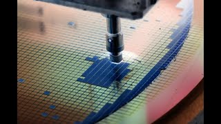
Role of Etching and Deposition
🔒 Unlock Audio Lesson
Sign up and enroll to listen to this audio lesson

Today, we're going to discuss the pivotal role of etching and deposition in semiconductor manufacturing. Can anyone tell me what we mean by etching?

Isn't etching the process of removing material to create patterns?
Exactly! And what about deposition?

That's when we add thin layers of material to a surface, right?
Correct! We can remember these two processes as 'E' for 'etching' and 'D' for 'deposition' — ED. Great job!

How do they work together?
They work in tandem! Etching defines the features, while deposition builds up the necessary layers to create functional devices. It's a dynamic duo!

That makes sense! So they are both critical to the fabrication process.
Exactly! Remember, their combined precision is essential for advanced semiconductor technologies.
In summary, etching defines features, while deposition constructs materials layers.
Importance of Precision
🔒 Unlock Audio Lesson
Sign up and enroll to listen to this audio lesson

Let's discuss precision. Why do you think it's critical in etching and deposition?
Maybe because we are working with nanoscale dimensions?
Exactly! At nanoscale, even tiny errors can propagate into significant defects in the final product. Can anyone list some challenges faced in achieving this precision?
I think it includes controlling etch rates and selectivity?
Right! And making sure that the processes do not damage the existing layers is also crucial. Let's remember EDS: Etching, Deposition, and Selectivity!
So, are there increasing demands for new technologies because of these challenges?
Precisely! As we move towards more complex devices, the demand for precise etching and deposition technologies increases.
In summary, precision and selectivity in these processes are vital for the integrity of nanoscale devices.
Future Directions
🔒 Unlock Audio Lesson
Sign up and enroll to listen to this audio lesson
Let's look towards the future. What do you think are the future directions for etching and deposition?
Maybe developing cheaper processes or new materials?
Good thought! Additionally, there’s a significant push towards 3D architectures. What impact could that have?
It means we need even more accurate etching to create vertical structures!
That's right! More advanced devices will demand the very best in both etching and deposition technologies.
So, this prepares us for new topics like CMP in the next chapter?
Exactly! CMP is crucial for achieving the necessary flat surfaces essential for multi-layer integration. In summary, the future lies in precision and adaptability.
Introduction & Overview
Read summaries of the section's main ideas at different levels of detail.
Quick Overview
Standard
In conclusion, etching and deposition processes are foundational to nanoscale patterning and integration in semiconductor manufacturing. With the growing complexity and precision needed for advancing circuit designs, these technologies are essential for creating high-aspect-ratio structures and preparing for the next topics, Chemical-Mechanical Planarization, and Surface Preparation.
Detailed
Conclusion
Etching and deposition processes are central to the development of semiconductor devices. This chapter has explored how these two mechanisms work in tandem to facilitate nanoscale patterning and the integration of materials. As manufacturing techniques evolve, there’s an increasing emphasis on achieving greater precision, particularly with high-aspect-ratio structures and complex 3D architectures. These advancements highlight the importance of continued innovation in etching and deposition processes.
Furthermore, they lay the groundwork for subsequent chapters where we will delve into Chemical-Mechanical Planarization (CMP) and Surface Preparation. These processes are vital for achieving flat, defect-free surfaces necessary for multilayer device integration. Understanding these concepts is essential for anyone looking to excel in semiconductor manufacturing technology.
Youtube Videos


Audio Book
Dive deep into the subject with an immersive audiobook experience.
Importance of Etching and Deposition
Chapter 1 of 3
🔒 Unlock Audio Chapter
Sign up and enroll to access the full audio experience
Chapter Content
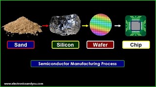
Etching and deposition are at the heart of nanoscale patterning and material integration in semiconductor manufacturing.
Detailed Explanation
This chunk emphasizes that etching and deposition are crucial processes in semiconductor manufacturing. They are responsible for creating and integrating nanoscale patterns and materials, which are essential for developing integrated circuits. These processes work together to shape the architecture of semiconductor devices at incredibly small sizes.
Examples & Analogies
Think of etching like sculpting a statue from a large block of stone, where you remove unwanted material to reveal a shape. Similarly, deposition is like adding layers of paint to enhance the sculpture, creating different features and finishes that serve a specific purpose.
Advancements in Semiconductor Manufacturing
Chapter 2 of 3
🔒 Unlock Audio Chapter
Sign up and enroll to access the full audio experience
Chapter Content
The transition to high-aspect-ratio structures, 3D architectures, and multi-patterning has pushed these processes toward greater precision and complexity.
Detailed Explanation
This chunk discusses the recent advancements in semiconductor technology, specifically focusing on high-aspect-ratio structures and 3D architectures. These advancements require etching and deposition processes to be more precise and complex than before, allowing manufacturers to create more efficient and powerful semiconductor devices. The mention of multi-patterning indicates techniques that allow for more patterns to be established on chips, increasing their functionality.
Examples & Analogies
Imagine a cake with multiple layers, where each layer has intricate designs. Just as a baker needs precision to create beautiful layers and patterns without collapsing the cake, semiconductor manufacturers need advanced techniques to ensure that the structures they create are both precise and able to support complex functionalities.
Looking Ahead
Chapter 3 of 3
🔒 Unlock Audio Chapter
Sign up and enroll to access the full audio experience
Chapter Content
In the next chapter, we will explore Chemical-Mechanical Planarization (CMP) and Surface Preparation, which ensure a flat, defect-free surface for multilayer integration.
Detailed Explanation
This chunk serves as a transition to the upcoming chapter, highlighting the importance of Chemical-Mechanical Planarization (CMP) and Surface Preparation in the semiconductor manufacturing process. These steps ensure that the surfaces on which subsequent layers are deposited are smooth and free of defects, which is vital for the performance and reliability of integrated circuits.
Examples & Analogies
Think of preparing the surface of a wall before painting. If the wall is not smooth and free from imperfections, the paint job will look uneven and unprofessional. Similarly, in semiconductor manufacturing, a flat and well-prepared surface is essential for successfully integrating multiple layers without issues.
Key Concepts
-
Nanoscale Patterning: The process of creating extremely small features in semiconductor manufacturing.
-
Material Integration: The combination of various materials in producing semiconductor devices.
-
3D Architectures: Enhanced designs that utilize three-dimensional structures in semiconductor devices.
Examples & Applications
An example of etching is using Reactive Ion Etching (RIE) to create precise patterns needed for modern CPUs.
Deposition can be exemplified through Atomic Layer Deposition (ALD), which is used to deposit thin films of materials crucial for gate dielectrics.
Memory Aids
Interactive tools to help you remember key concepts
Rhymes
Etch and deposit, make it so, creating patterns in a flow.
Stories
Imagine two artists, one etching fine lines in a stone and the other layering colors on a canvas. Together they produce a stunning piece of art, much like how etching and deposition work in semiconductor manufacturing.
Memory Tools
To remember the process order: E for Etching, D for Deposition — 'Every Detail Matters.'
Acronyms
Remember EDP
Etching
Deposition
Precision.
Flash Cards
Glossary
- Etching
The process of selectively removing materials to create patterns on semiconductor wafers.
- Deposition
The application of thin layers of material onto a substrate in semiconductor manufacturing.
- Precision
The degree of accuracy in maintaining the desired conditions during etching and deposition processes.
- High Aspect Ratio
The ratio of vertical dimension to horizontal dimension in a feature of a semiconductor device.
- 3D Architectures
Complex designs in semiconductor manufacturing that utilize three dimensions for device functionality.
Reference links
Supplementary resources to enhance your learning experience.