
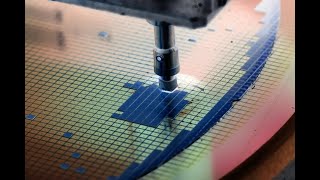
Main Deposition Techniques
Interactive Audio Lesson
Listen to a student-teacher conversation explaining the topic in a relatable way.
Understanding Physical Vapor Deposition (PVD)
🔒 Unlock Audio Lesson
Sign up and enroll to listen to this audio lesson

Today, we're diving into Physical Vapor Deposition, or PVD. It’s a process where materials are vaporized in a vacuum and then deposited on the wafer.

What kind of materials are typically used with PVD?
Great question! Common materials include Aluminum, Titanium, and Tungsten. Remember the acronym 'ATW' to help you recall these materials.

How does PVD differ from other deposition methods?
PVD is physical in nature, unlike Chemical Vapor Deposition, which involves chemical reactions. Can anyone tell me an example of a PVD application?

Coating metal layers for interconnects?
Exactly! PVD is often used for applying metal layers where conductivity is key. Let's recap: PVD vaporizes material in a vacuum to deposit layers for functionality.
Examining Chemical Vapor Deposition (CVD)
🔒 Unlock Audio Lesson
Sign up and enroll to listen to this audio lesson

Moving on, let's talk about Chemical Vapor Deposition, or CVD. This process uses gases to create films on the wafer.

What types of materials do we typically use in CVD?
In CVD, you often find materials like Silicon Dioxide and Silicon Nitride. Think of the acronym 'SiSiN' for Silicon films.
How is CVD beneficial compared to other methods?
CVD is advantageous because it can create uniform films even on complex surfaces. Why is uniformity important?
To ensure consistent electrical properties across devices?
Exactly right! Consistent layers help in achieving reliable circuit performance.
Exploring Atomic Layer Deposition (ALD)
🔒 Unlock Audio Lesson
Sign up and enroll to listen to this audio lesson
Now let's explore Atomic Layer Deposition, or ALD. This technique is known for its atomic-scale precision.
What makes ALD different from CVD or PVD?
ALD deposits material one atomic layer at a time—this self-limiting process ensures exact thickness control. Can anyone think of what materials ALD is used for?
High-k oxides?
Correct! ALD is ideal for high-k materials used in advanced transistors. So remember, atomically precise means better control over electronic properties!
Practical Applications of Spin Coating
🔒 Unlock Audio Lesson
Sign up and enroll to listen to this audio lesson
Finally, let's discuss Spin Coating. This method is primarily used for applying photoresists.
How does the spin coating process work?
In spin coating, a liquid material is deposited on the wafer and spun to spread it evenly. Remember the phrase 'Spin for Thin' to recall this process!
Why is it important to have a thin layer?
A thin layer allows for precise patterning during lithography. Can someone summarize how spin coating contributes to semiconductor processes?
It helps create uniform layers necessary for defining circuit features.
Perfect! Spin Coating is crucial for achieving the desired pattern definitions required in fabrication.
Introduction & Overview
Read summaries of the section's main ideas at different levels of detail.
Quick Overview
Standard
The section provides an overview of various deposition methods, including Physical Vapor Deposition (PVD), Chemical Vapor Deposition (CVD), Plasma-Enhanced CVD (PECVD), Atomic Layer Deposition (ALD), and Spin Coating, along with their typical materials and applications in semiconductor processes.
Detailed
Main Deposition Techniques
In semiconductor manufacturing, deposition processes are essential for creating functional layers on wafers. This section focuses on the main deposition techniques:
- Physical Vapor Deposition (PVD): This technique involves the vaporization of material in a vacuum, which then condenses on the wafer surface. Common materials used include Aluminum (Al), Titanium (Ti), and Tungsten (W).
- Chemical Vapor Deposition (CVD): In this method, gaseous reactants interact on the wafer to form a solid film. Typical materials deposited using CVD include Silicon Dioxide (SiO₂), Silicon Nitride (SiN), and polysilicon.
- Plasma-Enhanced CVD (PECVD): This variant of CVD operates at lower temperatures using plasma to enhance the reaction rates, making it suitable for low-k dielectrics.
- Atomic Layer Deposition (ALD): ALD features self-limiting reactions that allow for precise layer-by-layer deposition of materials, particularly useful for high-k oxides and Titanium Nitride (TiN).
- Spin Coating: Generally used for depositing photoresists or polymer layers, spin coating involves applying a liquid material to the wafer that is then spun to achieve a uniform thickness.
Each technique serves a distinct purpose in the semiconductor fabrication process, contributing to the comprehensive architecture of integrated circuits.
Youtube Videos


Audio Book
Dive deep into the subject with an immersive audiobook experience.
Introduction to Deposition Techniques
Chapter 1 of 6
🔒 Unlock Audio Chapter
Sign up and enroll to access the full audio experience
Chapter Content
Deposition builds functional layers required for:
● Transistors (gate oxide, metal contacts)
● Interconnects (metal layers)
● Isolation (dielectric barriers)
Detailed Explanation
Deposition techniques are essential in semiconductor manufacturing as they create the necessary layers that make up integrated circuits. These layers can be categorized as follows:
1. Transistors: These devices require layers for gate oxide, which is essential for controlling the flow of electrical current, and metal contacts that connect the transistors to the circuitry.
2. Interconnects: Layers of metal are deposited to create connections between different components in a microchip, allowing for communication across the device.
3. Isolation: Dielectric barriers are deposited to electrically isolate different components to prevent cross-talk and ensure proper functioning.
Examples & Analogies
Think of a multi-layer cake, where each layer has a specific flavor and purpose. Just as a cake needs different layers to create a harmonious taste experience, semiconductor devices require distinct layers to function effectively in processing and managing electrical signals.
Physical Vapor Deposition (PVD)
Chapter 2 of 6
🔒 Unlock Audio Chapter
Sign up and enroll to access the full audio experience
Chapter Content
Technique Description Typical Materials
Physical Vapor Deposition Material vaporized in vacuum and Al, Ti, W
deposited
Detailed Explanation
Physical Vapor Deposition, or PVD, is a process that creates thin films by vaporizing a solid material in a vacuum environment. Here's how it works:
1. A target material such as aluminum (Al), titanium (Ti), or tungsten (W) is heated until it vaporizes.
2. The vapor then travels through the vacuum and deposits itself onto the substrate (the surface where the layer is being created).
3. This technique is crucial for creating durable and conductive layers used in a variety of semiconductor applications.
Examples & Analogies
Imagine a magician pulling silk scarves from a hat. The scarves represent the material being vaporized in PVD. Just as the magician skillfully directs the scarves to create a beautiful pattern, PVD ensures the material deposits evenly and precisely on the wafer.
Chemical Vapor Deposition (CVD)
Chapter 3 of 6
🔒 Unlock Audio Chapter
Sign up and enroll to access the full audio experience
Chapter Content
Technique Description Typical Materials
Chemical Vapor Gases react on wafer to form a film SiO₂, SiN, polysilicon
Deposition (CVD)
Detailed Explanation
Chemical Vapor Deposition, commonly known as CVD, is a chemical process used to produce thin films. Here’s a breakdown of how it works:
1. Gases containing the desired elements are introduced to the surface of the wafer.
2. These gases undergo a chemical reaction, typically when heated, resulting in a solid film being deposited on the surface of the wafer.
3. Materials often created using CVD include silicon dioxide (SiO₂), silicon nitride (SiN), and polysilicon, all of which are crucial for the function of integrated circuits.
Examples & Analogies
Think of CVD like baking bread. The ingredients (gases) mix in the oven (wafer) and react with heat to form a delicious loaf (thin film). Just as the right combination of ingredients is vital for a perfect loaf, choosing the appropriate gases is crucial for successful CVD deposition.
Plasma-Enhanced CVD (PECVD)
Chapter 4 of 6
🔒 Unlock Audio Chapter
Sign up and enroll to access the full audio experience
Chapter Content
Technique Description Typical Materials
Plasma-Enhanced CVD CVD at lower temperature using Low-k dielectrics
plasma
Detailed Explanation
Plasma-Enhanced Chemical Vapor Deposition, or PECVD, is a variation of CVD that uses plasma to enhance the chemical reaction occurring on the wafer. This allows the process to be conducted at lower temperatures compared to traditional CVD. Here's how it works:
1. Plasma is generated using gases, which ionizes the gas molecules.
2. This energized state aids in the deposition of materials at lower temperatures, which is beneficial for heat-sensitive substrates.
3. PECVD is commonly used to deposit low-k dielectrics, which are essential for reducing capacitive coupling in interconnects.
Examples & Analogies
Think of PECVD like using a cold oven to cook. Instead of requiring high heat, the cold oven uses a different cooking method that allows for tasty results without the risk of burning delicate ingredients. Similarly, PECVD enables the formation of thin layers without damaging sensitive substrates.
Atomic Layer Deposition (ALD)
Chapter 5 of 6
🔒 Unlock Audio Chapter
Sign up and enroll to access the full audio experience
Chapter Content
Technique Description Typical Materials
Atomic Layer Deposition Self-limiting chemical reactions High-k oxides, TiN
(ALD) layer-by-layer
Detailed Explanation
Atomic Layer Deposition, or ALD, is a sophisticated technique used for applying extremely thin films in a highly controlled manner. The process works as follows:
1. The wafer is exposed to a precursor A, which chemically binds to the surface.
2. After a brief exposure, any excess material is purged away.
3. Then, precursor B is introduced, which reacts with precursor A, forming a second layer.
4. This cycle can be repeated to achieve atomic-scale control over film thickness, making ALD ideal for applications requiring precise layer thicknesses, such as high-k dielectrics and titanium nitride (TiN).
Examples & Analogies
ALD can be compared to building a carefully balanced stack of LEGO bricks, where you add one brick at a time with precision. Just as each LEGO piece snugly fits into place, ALD ensures that each layer is perfectly formed and evenly applied to achieve the desired structural integrity.
Spin Coating
Chapter 6 of 6
🔒 Unlock Audio Chapter
Sign up and enroll to access the full audio experience
Chapter Content
Technique Description Typical Materials
Spin Coating Used mainly for photoresist or Resist, planarization
polymer deposition layers
Detailed Explanation
Spin Coating is a process primarily used for applying thin layers of photoresist or polymer materials onto a wafer. Here's how it operates:
1. A small amount of liquid photoresist is placed at the center of the wafer.
2. The wafer is then rapidly spun. The centrifugal force spreads the liquid evenly across the surface.
3. As the wafer spins, a thin layer forms, which can then be cured through processes like baking. This technique is crucial in photolithography, where it creates the foundation for defining patterns on the wafer.
Examples & Analogies
Think of spin coating like icing a cake. When you pour icing onto the center of the cake and spin it, the icing spreads evenly across the surface. In the same way, spin coating ensures that the photoresist layer is uniformly applied, creating the necessary base for patterning.
Key Concepts
-
Physical Vapor Deposition (PVD): Vaporizes materials in a vacuum to coat substrates with a uniform film.
-
Chemical Vapor Deposition (CVD): Uses gaseous precursors to deposit solid layers on substrates.
-
Atomic Layer Deposition (ALD): Achieves layer-by-layer films with atomic precision.
-
Plasma-Enhanced CVD (PECVD): Employs plasma to facilitate low-temperature deposition.
-
Spin Coating: Applications of liquids through rapid spinning for creating uniform layers.
Examples & Applications
Photoresist application in semiconductor processing through spin coating.
Using PVD to deposit aluminum layers for interconnects.
Memory Aids
Interactive tools to help you remember key concepts
Rhymes
Layers of vapor, let them flow, PVD is where thin films grow.
Stories
In a factory, two friends, PVD and CVD, learn to create perfect layers. PVD vaporizes materials, while CVD combines gases, showing their unique trades.
Memory Tools
To remember deposition methods: PVD, CVD, PECVD, ALD, think 'Pretty Cool Processes Always Delight'.
Acronyms
PVD - Physical Vapor Deposition, CVD - Chemical Vapor Deposition.
Flash Cards
Glossary
- Physical Vapor Deposition (PVD)
A deposition method where material is vaporized in a vacuum to create films on a substrate.
- Chemical Vapor Deposition (CVD)
A technique where gases react chemically on a substrate to form solid films.
- Atomic Layer Deposition (ALD)
A process that deposits thin films layer by layer, achieving atomic-level precision.
- PlasmaEnhanced CVD (PECVD)
An adapted CVD process that uses plasma to lower the temperature of film formation.
- Spin Coating
A method used to apply uniform layers of liquid materials to substrates through rotation.
Reference links
Supplementary resources to enhance your learning experience.