
Analysis and Observations
Interactive Audio Lesson
Listen to a student-teacher conversation explaining the topic in a relatable way.
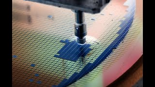
Importance of Etching
🔒 Unlock Audio Lesson
Sign up and enroll to listen to this audio lesson

Let's explore the importance of etching. Why do you think etching is crucial in defining features on a semiconductor?

I think it's because etching helps remove unwanted material to create space for the structure.

Yeah, but it also helps achieve those intricate pattern designs, right?
Exactly! Etching is key to precision in feature definition. We often consider 'selectivity'— the ability to remove one material without affecting others. Remember the mnemonic 'Selectivity Saves Structures' to help remember that!
Dry Etching Advantages
🔒 Unlock Audio Lesson
Sign up and enroll to listen to this audio lesson

Great discussion on etching! Now, what about dry etching? What are some advantages it has?

It allows for vertical profiles and precise feature control!

But doesn't it also cause surface damage sometimes?
Correct! While dry etching is advantageous, we must be wary of surface damage. Think of it as a balance: 'Precision vs. Protection.'
Atomic Layer Deposition (ALD)
🔒 Unlock Audio Lesson
Sign up and enroll to listen to this audio lesson
Now, let's focus on deposition processes, specifically ALD. What makes ALD special for semiconductor applications?
It creates atomic-scale uniform layers, which is essential for some components?
Yeah! Especially for high-k materials used in advanced devices.
Precisely! Remember, 'ALD = Atomic Layer Duty'. This helps reinforce its function in achieving uniform film thickness essential for performance!
Process Selection Criteria
🔒 Unlock Audio Lesson
Sign up and enroll to listen to this audio lesson
When selecting between etching and deposition processes, what factors should we consider?
Material compatibility definitely plays a big role.
And the size of the feature we want to create!
Exactly, as well as temperature limits and throughput needs. Remember the acronym 'M-F-T-T' for Material, Feature, Temperature, and Throughput considerations, that will help you remember these essentials when making choices.
Introduction & Overview
Read summaries of the section's main ideas at different levels of detail.
Quick Overview
Standard
Here, we delve into the importance of etching and deposition processes in semiconductor manufacturing, detailing their roles in defining features and building functional layers on a wafer. Considerations such as material compatibility and damage control are also discussed.
Detailed
Detailed Summary
In semiconductor manufacturing, processes such as etching and deposition are fundamental in shaping and constructing integrated circuits. This section discusses the essential role of etching in defining intricate features and the critical function of deposition in forming structural and functional layers on the semiconductor wafer.
- Key Roles: Etching allows for precise feature definition, while deposition techniques create various thin layers such as conductive, insulating, and barrier materials.
- Dry Etching Advantages: The dry etching process provides better control over vertical profiles and fine features; however, it may lead to surface damage, an important consideration during device fabrication.
- Atomic Layer Deposition (ALD): Recognized for its atomic-scale uniformity, ALD proves advantageous for specialized applications like gate dielectrics and high-k materials, making it ideal for advanced semiconductor devices.
- Process Selection Criteria: When choosing between etching and deposition processes, factors such as material compatibility, feature size, temperature limits, and throughput requirements are vital and need to be meticulously considered to ensure the material integrity and device performance.
Youtube Videos


Audio Book
Dive deep into the subject with an immersive audiobook experience.
Role of Etching and Deposition
Chapter 1 of 4
🔒 Unlock Audio Chapter
Sign up and enroll to access the full audio experience
Chapter Content
● Etching is key to defining features, while deposition creates functional and structural layers.
Detailed Explanation
In semiconductor manufacturing, etching and deposition play fundamental roles. Etching is the process that helps carve out the precise patterns and shapes needed on the surface of the semiconductor wafers. Meanwhile, deposition is responsible for adding layers of materials that are necessary for the components to function properly, like insulating layers for transistors or interconnects.
Examples & Analogies
Think of etching as sculpting a statue from a block of marble; the sculptor removes material to reveal the shape underneath. Deposition, on the other hand, is like applying paint to the sculpture — it adds color and protective layers that are essential for the sculpture's final appearance and longevity.
Benefits and Challenges of Dry Etching
Chapter 2 of 4
🔒 Unlock Audio Chapter
Sign up and enroll to access the full audio experience
Chapter Content
● Dry etching allows vertical profiles and fine feature control but may cause surface damage.
Detailed Explanation
Dry etching uses gases or plasma to remove materials in a controlled manner, allowing for precise, vertical structures needed for modern semiconductor devices. However, one must be cautious as this method can also damage the remaining surfaces if not carefully controlled, leading to defects that might affect the performance of the device.
Examples & Analogies
Imagine using a high-powered vacuum cleaner to clean corners of a room. It gets into tight spaces effectively (similar to how dry etching can create precise patterns), but if you're not careful, it may suck up or damage surrounding items (representing potential surface damage).
Advantages of Atomic Layer Deposition (ALD)
Chapter 3 of 4
🔒 Unlock Audio Chapter
Sign up and enroll to access the full audio experience
Chapter Content
● ALD offers atomic-scale uniformity — ideal for gate dielectrics and high-k materials.
Detailed Explanation
Atomic Layer Deposition (ALD) is a technique that allows for the deposition of materials one atomic layer at a time. This results in highly uniform and conformal layers, which is particularly advantageous for creating materials needed in modern electronics, such as gate dielectrics in transistors. ALD’s precision ensures that layers are consistently thin and evenly distributed, vital in advanced semiconductor design.
Examples & Analogies
Consider frosting a cake. If you use a thin spreader and apply frosting layer by layer, you ensure each layer is consistent and smooth (just like ALD). In contrast, if you glob on frosting in large amounts, you may create uneven layers (analogous to less controlled deposition techniques).
Factors Influencing Process Choices
Chapter 4 of 4
🔒 Unlock Audio Chapter
Sign up and enroll to access the full audio experience
Chapter Content
● The choice of process depends on:
○ Material compatibility
○ Feature size
○ Temperature budget
○ Throughput requirements.
Detailed Explanation
When deciding on an etching or deposition process, several important factors must be considered. Material compatibility ensures that the chosen process does not damage the materials involved. Feature size dictates how fine or coarse the patterns can be. The temperature budget relates to how much heat the materials can withstand during processing, and throughput refers to the speed and efficiency of the process. These factors all combine to guide engineers in selecting the most suitable method for their needs.
Examples & Analogies
Choosing the right path for a road trip can depend on various factors — like the type of car you have (material compatibility), the road conditions (feature size), the weather (temperature budget), and how quickly you want to reach your destination (throughput requirements). Making informed choices ensures a smooth journey.
Key Concepts
-
Etching is critical for defining features in semiconductor devices.
-
Deposition processes create functional layers necessary for device performance.
-
Consider material compatibility and feature size when selecting processes.
Examples & Applications
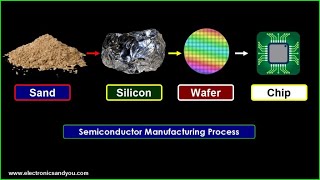
Etching is used to carve out intricate patterns on a silicon wafer, which are essential for integrated circuits.
ALD is employed to ensure uniform gate oxides, critical for the performance of transistors in modern microchips.
Memory Aids
Interactive tools to help you remember key concepts
Rhymes
Etch and define, features align; Deposition's layers so fine.
Stories
Imagine a sculptor carefully chiseling away stone, defining each detail, just like etching carves intricate patterns on a wafer.
Memory Tools
Remember 'E-D, A-Precision' for Etching-Deposition and the need for precision.
Acronyms
Use 'MFTT' to recall Material compatibility, Feature size, Temperature, and Throughput for process choice.
Flash Cards
Glossary
- Etching
A process used in semiconductor manufacturing to remove material and define features on the wafer.
- Deposition
The deposition process involves applying thin layers of materials onto the semiconductor wafer.
- Selectivity
The characteristic that allows the removal of one material without affecting others.
- Anisotropy
Directional etching, which is essential for maintaining vertical profiles during the etching process.
- Atomic Layer Deposition (ALD)
A deposition technique that builds layers atom by atom, providing precise control over film thickness.
- Dry Etching
Etching that uses plasma or gases in a vacuum to remove material, allowing for greater precision.
Reference links
Supplementary resources to enhance your learning experience.