
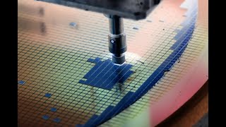
Step 1: Etching Processes
Interactive Audio Lesson
Listen to a student-teacher conversation explaining the topic in a relatable way.
Types of Etching
🔒 Unlock Audio Lesson
Sign up and enroll to listen to this audio lesson

Today, we're going to discuss the types of etching processes used in semiconductor manufacturing. Can anyone tell me what wet etching is?

Wet etching involves using liquid chemicals to dissolve materials.
That's right! Wet etching is simpler but tends to be isotropic. Now, can someone explain dry etching?

Dry etching uses plasma or gases and can be more precise.
Excellent! Dry etching is often anisotropic, which is important for maintaining vertical profiles in patterns. Can anyone tell me about reactive ion etching?

RIE combines plasma with directional ion bombardment for more precise etching.
Great! RIE is widely used in advanced semiconductor nodes due to its precision. Remember the acronym WDR for Wet, Dry, and Reactive ion etching!
To summarize, we covered wet, dry, and RIE etching processes, each with its pros and cons.
Key Properties of Etching
🔒 Unlock Audio Lesson
Sign up and enroll to listen to this audio lesson

Let's dive into the key properties of etching processes. Can someone explain what selectivity means in this context?

Selectivity is when one material is etched away while leaving other materials unharmed.
Exactly! Selectivity is vital for working with multi-layer structures. Now, how about anisotropy?
Anisotropy refers to directional etching, which helps in forming features with vertical profiles.
Correct! Anisotropic etching is essential for fine features. And what does etch rate control refer to?
It's about controlling how quickly material is removed to maintain accuracy.
That's right! Always think of the 'S-A-R' acronym for Selectivity, Anisotropy, and Rate to remember these properties.
To summarize, we discussed selectivity, anisotropy, and etch rate control — critical properties that influence etching effectiveness.
Common Etch Chemistries
🔒 Unlock Audio Lesson
Sign up and enroll to listen to this audio lesson
Now, let's move on to the common etching chemistries. Can anyone identify the chemistry used for etching SiO₂?
CF₄ or CHF₃ is used for SiO₂!
Correct! What about Si₃N₄?
It's SF₆ or H₃PO₄ for etching Si₃N₄.
Exactly! And for aluminum, what chemistries do we need?
We need Cl₂ or BCl₃ plasmas to etch aluminum.
Great job! Remembering these chemistries can be essential in selecting the right process for different materials. Think of 'A-S-S' for Aluminum, Si₃N₄, and SiO₂ chemistries.
To summarize, we reviewed common etch chemistries for SiO₂, Si₃N₄, and aluminum.
Introduction & Overview
Read summaries of the section's main ideas at different levels of detail.
Quick Overview
Standard
In semiconductor manufacturing, etching is a pivotal process that selectively removes materials to create intricate designs on wafers. This section details various etching types, including wet and dry etching, alongside their key properties such as selectivity and anisotropy, while also listing common etching chemistries utilized for specific materials.
Detailed
Step 1: Etching Processes
In semiconductor manufacturing, etching is essential for forming precise patterns on wafers, involving the selective removal of materials defined in the lithography stage. This section delves into the different types of etching, key etching properties, and common etch chemistries.
Types of Etching
- Wet Etching: Utilizes chemical etchants in liquid form to dissolve materials. This method is simpler but typically isotropic, meaning it etches uniformly in all directions.
- Dry Etching: Employs plasma or gases in a vacuum environment to remove material with more precision, allowing for anisotropic etching, which is critical for maintaining vertical features and high resolution.
- Reactive Ion Etching (RIE): Combines the benefits of plasma and directional ion bombardment, making it suitable for advanced technology nodes requiring high precision.
Key Properties of Etching
- Selectivity: The ability to etch one material without affecting others, crucial for multi-layer structures.
- Anisotropy: Directional etching that helps achieve vertical profiles, crucial for forming fine features.
- Etch Rate Control: Essential for maintaining critical dimension accuracy, ensuring that features are precisely defined.
Common Etch Chemistries
- SiO₂: Typically etched using CF₄ or CHF₃.
- Si₃N₄: Etched with SF₆ or H₃PO₄.
- Aluminum: Requires Cl₂ or BCl₃ plasmas for effective etching.
Understanding these etching processes and their properties is fundamental for achieving the desired precision and performance in semiconductor devices.
Youtube Videos


Audio Book
Dive deep into the subject with an immersive audiobook experience.
Types of Etching
Chapter 1 of 3
🔒 Unlock Audio Chapter
Sign up and enroll to access the full audio experience
Chapter Content
Types of Etching:
| Type | Description | Use Case |
|---|---|---|
| Wet Etching | Chemical etchants dissolve materials in liquid phase. | Simpler, but isotropic |
| Dry Etching | Uses plasma or gases in vacuum to remove material. | Anisotropic, high-resolution |
| Reactive Ion Etching (RIE) | Combines plasma and directional ion bombardment. | Precise, used in advanced nodes |
Detailed Explanation
This chunk outlines the main types of etching used in semiconductor processes.
- Wet Etching: In this method, materials are dissolved by chemical solutions in a liquid state. This process is simpler but often results in isotropic etching, which means it removes material uniformly in all directions, making it less suitable for detailed patterns.
- Dry Etching: This technique utilizes the power of plasma or gases inside a vacuum chamber. It allows for anisotropic etching, meaning it can remove material in a directional manner, which is often necessary for creating sharp, vertical edges in semiconductor patterns.
- Reactive Ion Etching (RIE): RIE is a more advanced technique that merges the benefits of plasma etching and directionality. Ion bombardment with plasma helps achieve high precision, essential for the newest technology nodes in semiconductor fabrication.
Examples & Analogies
Think of wet etching as using a sponge to erase a chalkboard—wiping all the chalk off evenly everywhere. In contrast, dry etching is like using a precision eraser that can focus on specific areas, allowing you to create sharp lines and shapes, similar to how an artist might carefully remove paint from a canvas.
Key Properties of Etching
Chapter 2 of 3
🔒 Unlock Audio Chapter
Sign up and enroll to access the full audio experience
Chapter Content
Key Properties of Etching:
- Selectivity: Ability to remove one material without affecting others.
- Anisotropy: Directional etching, important for vertical profiles.
- Etch Rate Control: Vital for critical dimension accuracy.
Detailed Explanation
This chunk describes three essential properties that define etching processes:
- Selectivity: This refers to the capability of the etching process to selectively remove certain materials while leaving others intact. This is crucial in semiconductor manufacturing because different layers must be etched without damaging underlying materials.
- Anisotropy: Anisotropic etching means that the material is removed in a specific direction, which is particularly important when creating vertical profiles for features in the semiconductor. This prevents over-etching or under-etching on sides that could affect the performance of the components.
- Etch Rate Control: This property is vital for maintaining precise control over the dimensions of features created on the semiconductor. The etch rate determines how quickly material is removed and must be monitored to achieve the accuracy needed for modern electronic devices.
Examples & Analogies
Imagine using a sculpting tool to carve a statue. If your tool is precise (anisotropic), you can create detailed features without affecting other parts (selectivity), and you can decide how quickly to remove material depending on how intricate the design is (etch rate control).
Common Etch Chemistries
Chapter 3 of 3
🔒 Unlock Audio Chapter
Sign up and enroll to access the full audio experience
Chapter Content
Common Etch Chemistries:
- SiO₂: Etched with CF₄ or CHF₃.
- Si₃N₄: Etched using SF₆ or H₃PO₄.
- Aluminum: Requires Cl₂ or BCl₃ plasmas.
Detailed Explanation
This chunk lists specific chemicals and gases commonly used in the etching processes:
- SiO₂ (Silicon Dioxide): This material is often etched using CF₄ (Carbon Tetrafluoride) or CHF₃ (Trifluoromethane). These gases react with SiO₂, allowing it to be removed effectively.
- Si₃N₄ (Silicon Nitride): SF₆ (Sulfur Hexafluoride) and H₃PO₄ (Phosphoric Acid) are used to etch silicon nitride, enabling the creation of the necessary patterns on the semiconductor wafers.
- Aluminum: To etch aluminum layers, Cl₂ (Chlorine) or BCl₃ (Boron Trichloride) plasmas are typically employed. The choice of etch chemistry is important as it impacts the selectivity and precision of the etching process.
Examples & Analogies
Consider different types of paint strippers that work better on specific colors or surface materials. Similarly, each etch chemistry is specially designed to react with certain materials (like a tailored paint stripper) ensuring that the intended material is removed while protecting others from damage.
Key Concepts
-
Etching Types: Understanding the differences between wet, dry, and RIE etching methods.
-
Key Properties: Recognizing selectivity, anisotropy, and etch rate control as fundamentals in etching processes.
-
Chemistries: Being familiar with chemistries used for etching specific materials such as SiO₂, Si₃N₄, and aluminum.
Examples & Applications
Wet etching is commonly used for simpler materials where isotropic etching is sufficient, while dry etching is preferred for high-resolution features in integrated circuits.
Reactive Ion Etching is used in advanced semiconductor nodes to achieve vertical profiles and precise dimensions.
Memory Aids
Interactive tools to help you remember key concepts
Rhymes
Wet and dry, one is clear, with RIE, precision's near!
Stories
Imagine a sculptor carefully etching a statue; wet etching smoothens the surface, while dry etching sharpens the details, making each feature stand out.
Memory Tools
Remember 'S-A-R' for Selectivity, Anisotropy, and Rate in etching!
Acronyms
WDR stands for Wet, Dry, and Reactive ion etching processes!
Flash Cards
Glossary
- Wet Etching
A process using chemical etchants in a liquid phase to dissolve materials.
- Dry Etching
An etching process utilizing plasma or gases in a vacuum to selectively remove material.
- Reactive Ion Etching (RIE)
An advanced etching technique that combines plasma and directional ion bombardment.
- Selectivity
The ability to remove one material while leaving others intact.
- Anisotropy
Directional etching that helps achieve vertical profiles of features.
- Etch Rate Control
The ability to control the speed of material removal during the etching process.
Reference links
Supplementary resources to enhance your learning experience.