
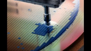
Types of Etching
Interactive Audio Lesson
Listen to a student-teacher conversation explaining the topic in a relatable way.
Wet vs. Dry Etching
🔒 Unlock Audio Lesson
Sign up and enroll to listen to this audio lesson

Today, we're diving into the main types of etching used in semiconductor manufacturing. Can anyone tell me the two primary categories?

Wet etching and dry etching, right?
Exactly! Wet etching uses liquid chemical etchants, which is simpler but results in isotropic etching, meaning it removes material uniformly in all directions. How about dry etching?

Dry etching uses plasma or gases, so it can achieve more precise, directional etching!
Great! Remember: Wet etching is isotropic, while dry etching is anisotropic. Can anyone think of situations where you'd prefer one over the other?

I think wet etching might be used for simpler patterns, while dry etching would be necessary for more detailed structures.
Exactly! Let's summarize: Wet etching is useful for basic applications, while dry etching is crucial for high-resolution and complex designs.
Understanding RIE
🔒 Unlock Audio Lesson
Sign up and enroll to listen to this audio lesson

Now, let's focus on Reactive Ion Etching, or RIE. Why do you think RIE is so important in semiconductor processes?

I heard it combines plasma and directional ion bombardment for very precise etching, right?
Exactly! RIE provides precision and is often used in advanced nodes. What is one of the main benefits of having such precise control?
It helps to maintain critical dimensions in very small features!
Correct! It's all about achieving accuracy at the nanoscale. And what do we need to keep in mind when using RIE?
We have to control etch rates and monitor selectivity to avoid damaging other materials on the wafer.
That's right! Remember: RIE is about precision and control—key for modern semiconductor manufacturing.
Etching Properties and Chems
🔒 Unlock Audio Lesson
Sign up and enroll to listen to this audio lesson
Let’s review some key properties of etching. Who can explain what selectivity in etching means?
Selectivity is the ability to remove one material without affecting others, right?
Spot on! Selectivity allows for precise patterning. What about anisotropy?
Anisotropy is the directional etching that creates vertical profiles.
Correct! Anisotropic etching is crucial for maintaining the intended structure in a device. Can anyone name a common chemistry used for etching?
CF₄ for SiO₂?
Yes! CF₄ and CHF₃ are commonly used. Remember these chemistries; they are crucial for effective etching!
Introduction & Overview
Read summaries of the section's main ideas at different levels of detail.
Quick Overview
Standard
The section provides a comprehensive overview of etching techniques such as wet etching, dry etching, and reactive ion etching. It discusses their functionalities, key properties like anisotropy and selectivity, and common chemistries employed for different materials.
Detailed
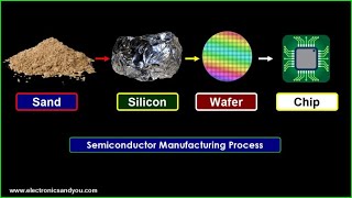
In semiconductor fabrication, etching is a critical process used to pattern materials on a wafer. This section describes three primary types of etching: Wet Etching, which employs chemical solutions to dissolve materials isotropically; Dry Etching, which utilizes gases or plasma in a vacuum to achieve anisotropic etching; and Reactive Ion Etching (RIE), which combines elements of both wet and dry etching for precise material removal. Key properties of etching include selectivity, which is the ability to target specific materials for removal without affecting others; anisotropy, which refers to directional etching for achieving vertical profiles; and etch rate control important for maintaining critical dimensions. Common chemistries include CF₄ or CHF₃ for SiO₂, SF₆ or H₃PO₄ for Si₃N₄, and Cl₂ or BCl₃ plasmas for aluminum. Understanding these techniques and properties is vital for achieving the desired features in semiconductor devices.
Youtube Videos


Audio Book
Dive deep into the subject with an immersive audiobook experience.
Wet Etching
Chapter 1 of 5
🔒 Unlock Audio Chapter
Sign up and enroll to access the full audio experience
Chapter Content
Wet Etching
Chemical etchants dissolve materials in liquid phase.
Use Case
Simpler, but isotropic.
Detailed Explanation
Wet etching is a process where chemicals in a liquid form dissolve specific materials from the surface of a semiconductor wafer. It is simpler in implementation than some other methods, making it accessible for various applications. However, one of its key characteristics is isotropy, meaning it removes material uniformly in all directions. This can be a limitation when creating fine features on microchips because it doesn't allow for precise shaping needed for modern semiconductors.
Examples & Analogies
Imagine pouring salt on a steak to Enhance its flavor. The salt dissolves in the juices and affects the steak uniformly, regardless of where the salt is placed. Similarly, wet etching dissolves material uniformly, which can sometimes lead to a lack of precision in the delicate structures required in microelectronics.
Dry Etching
Chapter 2 of 5
🔒 Unlock Audio Chapter
Sign up and enroll to access the full audio experience
Chapter Content
Dry Etching
Uses plasma or gases in vacuum to remove material.
Use Case
Anisotropic, high-resolution.
Detailed Explanation
Dry etching uses gases or plasmas in a vacuum environment, which allows for more controlled material removal. Unlike wet etching, it produces anisotropic results, meaning the etching occurs more in one direction than in others. This characteristic is crucial for achieving vertical profiles in microfabrications, necessary for advanced semiconductor technology. The high-resolution capability of dry etching makes it ideal for producing intricate patterns on a chip.
Examples & Analogies
Think of using a laser cutter to carve precise shapes from wood. The laser can cut straight down, creating clean, vertical edges that you couldn't achieve with a saw. Similarly, dry etching enables the precise manufacturing of small features on semiconductors, allowing for more complex designs.
Reactive Ion Etching (RIE)
Chapter 3 of 5
🔒 Unlock Audio Chapter
Sign up and enroll to access the full audio experience
Chapter Content
Reactive Ion Etching (RIE)
Combines plasma and directional ion bombardment.
Use Case
Precise, used in advanced nodes.
Detailed Explanation
Reactive Ion Etching (RIE) is an advanced form of dry etching that integrates both plasma etching and ion bombardment. It adds directionality to the etching process, improving precision and control, which is especially important for the latest technology nodes in semiconductor production. This process allows manufacturers to create detailed patterns while maintaining the integrity of the material beneath, achieving high fidelity in feature sizes.
Examples & Analogies
Imagine a sculptor who uses both a chisel and a sandblaster to shape a statue. The chisel can precisely carve out details, while the sandblaster uniformly smooths the surface. In RIE, the combination of plasma and ion bombardment allows for both precision and surface smoothing in etching processes.
Key Properties of Etching
Chapter 4 of 5
🔒 Unlock Audio Chapter
Sign up and enroll to access the full audio experience
Chapter Content
Key Properties of Etching
- Selectivity: Ability to remove one material without affecting others.
- Anisotropy: Directional etching, important for vertical profiles.
- Etch Rate Control: Vital for critical dimension accuracy.
Detailed Explanation
Understanding the key properties of etching is essential in semiconductor manufacturing. Selectivity ensures that only the target material is removed while leaving others intact, preserving the integrity of the structure. Anisotropy emphasizes the directional control needed to create distinct vertical patterns. Finally, controlling the etch rate allows for precise management of how much material is removed, which is crucial for maintaining critical dimensions on microchips.
Examples & Analogies
Consider carving a pumpkin for Halloween. If you want to create facial features without cutting through the entire pumpkin, you need to control how deep you carve (selectivity), make sure you're carving in a specific direction (anisotropy), and take care not to carve too quickly or deeply (etch rate control). These principles are the same in etching processes used in chip manufacturing.
Common Etch Chemistries
Chapter 5 of 5
🔒 Unlock Audio Chapter
Sign up and enroll to access the full audio experience
Chapter Content
Common Etch Chemistries
- SiO₂: Etched with CF₄ or CHF₃.
- Si₃N₄: Etched using SF₆ or H₃PO₄.
- Aluminum: Requires Cl₂ or BCl₃ plasmas.
Detailed Explanation
Different materials require specific chemical processes for effective etching. For instance, silicon dioxide (SiO₂) is typically etched with gases like CF₄ (tetrafluoromethane) or CHF₃ (trifluoroethane). For silicon nitride (Si₃N₄), good results are achieved using SF₆ (sulfur hexafluoride) or H₃PO₄ (phosphoric acid). Aluminum etching relies on Cl₂ (chlorine) or BCl₃ (boron trichloride) plasmas. Understanding the right chemistry for the material is crucial for successful etching and achieving the desired outcomes in semiconductor processing.
Examples & Analogies
Just like choosing the right cleaner for your car, where different materials require different products for optimal results, semiconductor manufacturing requires distinct chemicals tailored to the specific materials being etched. Using the correct chemical means more effective and efficient work.
Key Concepts
-
Wet Etching: Uses liquid chemicals for isotropic material removal.
-
Dry Etching: Involves plasma or gases for directional, high-resolution etching.
-
Reactive Ion Etching (RIE): Combines features of wet and dry etching for precision.
-
Etcing Properties: Key properties include selectivity and anisotropy.
-
Common Chemistries: Specific chemicals used for etching various materials.
Examples & Applications
Using CF₄ for etching SiO₂ in dry etching processes.
Utilizing a wet etching process for simpler patterns like pads on a wafer.
Memory Aids
Interactive tools to help you remember key concepts
Rhymes
Wet etch, dry etch, all for the best, rock-solid patterns that pass the test!
Stories
Imagine a sculptor using water to smooth a round stone (wet etching) versus a saw to carve sharp lines (dry etching). Each method leads to a different final look!
Memory Tools
To remember types of etching: WED - Wet, Etching, Dry.
Acronyms
SAND - Selectivity, Anisotropy, Nitrogen chemistry, Dry etching.
Flash Cards
Glossary
- Etching
A process used to remove material from the surface of a semiconductor wafer to create patterns.
- Wet Etching
A type of etching that uses liquid chemical etchants to dissolve materials.
- Dry Etching
A method of etching that uses plasma or gases in a vacuum to remove material with directional control.
- Reactive Ion Etching (RIE)
A technique combining the properties of both wet and dry etching for high-precision material removal.
- Selectivity
The ability to selectively remove one material while preserving others during the etching process.
- Anisotropy
Directional etching that enables the creation of vertical profiles in the materials.
Reference links
Supplementary resources to enhance your learning experience.