
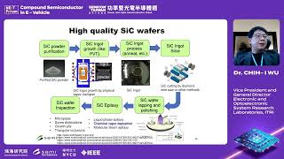
Cleanroom and Process Requirements
Interactive Audio Lesson
Listen to a student-teacher conversation explaining the topic in a relatable way.
Importance of Cleanroom Environments
🔒 Unlock Audio Lesson
Sign up and enroll to listen to this audio lesson

Today, we're going to discuss the role of cleanroom environments in semiconductor fabrication. Why do you think a cleanroom environment is important for processes like these?

I guess if there’s dust or dirt, it could mess with the materials we are using.
Exactly! In semiconductor fabrication, even tiny particles can cause performance issues. A cleanroom classified as Class 100 ensures that no more than 100 particles of size 0.5 micrometers are present in the air. Why do you think contamination control is emphasized?

Because materials like oxygen and metal can degrade the performance of the semiconductors!
Correct! Metal and oxygen contaminations can significantly impair electrical and optical properties. Let's remember that by using the acronym 'COM' — Contamination, Oxygen, Metal. Now, can anyone explain what quantum wells and heterostructures are and why their thickness control is crucial?

Quantium wells and heterostructures are layers that help control electronic properties. If their thickness isn't correct, then the device won't work properly!
Exactly! Precision in controlling these thicknesses at a nanometer scale is fundamental. In summary, cleanroom environments and stringent contamination control are vital for achieving high-performance semiconductors.
Layer Thickness Control
🔒 Unlock Audio Lesson
Sign up and enroll to listen to this audio lesson

Now let's explore layer thickness control more specifically. How do you think layer thickness influences semiconductor functionality?

If it's too thick or too thin, the electric and optical properties might change, right?
Correct! The control over layer thickness, especially down to nanometer precision, directly affects the electronic and optical properties. This control is vital for devices like lasers and LEDs. Remember, precise control means better device performance. Can anyone name an application where thickness control is particularly critical?
In quantum dot lasers, I think controlling the thickness of the layers can help maximize efficiency!
Exactly right! In quantum dot structures, the layer thickness determines the energy levels and thus the efficiency of the laser. This reinforces why we need strict cleanroom standards for achieving such precision.
Introduction & Overview
Read summaries of the section's main ideas at different levels of detail.
Quick Overview
Standard
In the fabrication of compound semiconductors, maintaining a cleanroom environment with a classification of Class 100 or better is essential to prevent contamination. Metal and oxygen impurities can degrade device performance, necessitating strict contamination control procedures, alongside precise control over layer thickness, particularly in quantum wells and heterostructures.
Detailed
Cleanroom and Process Requirements
The fabrication of compound semiconductors necessitates high standards of cleanliness, as even minute contamination can significantly affect device performance. A cleanroom classified as Class 100 is required, meaning that no more than 100 particles of size 0.5 micrometers or larger are allowed per cubic foot of air. This stringent requirement highlights the sensitive nature of compound semiconductor materials and their reliance on pristine conditions for growth and processing.
To ensure optimal performance, strict contamination control measures must be in place to prevent metal and oxygen contaminations, both of which can degrade electrical and optical properties. Moreover, the precision in controlling layer thickness in nanometer scales is critical when dealing with structures like quantum wells and heterostructures. Such precision enables the fine-tuning of the electronic and optical characteristics of semiconductors, proving vital in producing high-performance devices. Overall, the cleanroom and process requirements are integral to achieving the significant advancements in compound semiconductor technology.
Youtube Videos
Audio Book
Dive deep into the subject with an immersive audiobook experience.
Cleanroom Environment
Chapter 1 of 3
🔒 Unlock Audio Chapter
Sign up and enroll to access the full audio experience
Chapter Content
● Cleanroom Environment: Class 100 or better
Detailed Explanation
A cleanroom is a controlled environment where the levels of pollutants and contaminants are minimized. A 'Class 100' cleanroom means that it allows a maximum of 100 particles larger than 0.5 µm per cubic foot of air. This cleanliness is crucial when fabricating devices, especially semiconductors, because even tiny particles can cause defects in the material being created. The more stringent the class, the fewer contaminations allowed, which directly affects the quality of the semiconductor products.
Examples & Analogies
Think of a cleanroom as a sterile operating room in a hospital. Just like surgeons need a clean environment to perform surgeries and avoid infections, semiconductor manufacturers need a cleanroom to ensure that their devices are free from contaminants that could impair functionality.
Contamination Control
Chapter 2 of 3
🔒 Unlock Audio Chapter
Sign up and enroll to access the full audio experience
Chapter Content
● Contamination Control: Metal and oxygen contamination can degrade performance
Detailed Explanation
Contamination control in semiconductor fabrication involves keeping the environment free from unwanted materials, such as metals and oxygen. These contaminants can interfere with the function of electronic components, leading to lower performance or failure. Strict protocols are in place to ensure that no impurities enter the cleanroom, including air filters, gowning procedures, and regular monitoring of air quality.
Examples & Analogies
This is similar to baking a cake; if you accidentally add salt instead of sugar, the cake won’t taste right. Likewise, even minute amounts of contaminants in semiconductor layers can result in significant performance issues for the final device.
Layer Thickness Control
Chapter 3 of 3
🔒 Unlock Audio Chapter
Sign up and enroll to access the full audio experience
Chapter Content
● Layer Thickness Control: Nanometer-scale control essential in quantum wells and heterostructures
Detailed Explanation
In semiconductor manufacturing, controlling the thickness of layers is critically important, especially at the nanometer scale. Quantum wells and heterostructures are specific designs where the thickness of these layers must be precisely controlled to achieve the desired electrical and optical properties. Variations in thickness can lead to variations in electronic behavior, impacting the device's performance. Advanced technologies and techniques such as atomic layer deposition (ALD) are commonly used to achieve this precision.
Examples & Analogies
Think of a sandwich: if you make a sandwich with a very thick layer of mustard, it may overpower the other flavors, while too little can make it dry. In the same way, getting the thickness just right in semiconductor layers is critical for balancing the properties and achieving the best performance.
Key Concepts
-
Cleanroom: A controlled environment that limits airborne particles.
-
Class 100: A standard for cleanroom air cleanliness.
-
Contamination Control: Essential measures to prevent performance degradation of semiconductors.
-
Layer Thickness Control: Critical for achieving desired electronic and optical properties.
-
Quantum Wells: Layers that confine charge carriers to create distinct energy states.
-
Heterostructures: Stacked layers of different materials tailored for specific electronic properties.
Examples & Applications
The need for a Class 100 cleanroom in the production of LEDs, where even small particles could affect light output.
Layer thickness control in quantum wells is vital for ensuring the desired electronic properties are achieved in semiconductor lasers.
Memory Aids
Interactive tools to help you remember key concepts
Rhymes
In a cleanroom so tight, less than 100 in sight, to keep the devices right, for performance in flight.
Stories
Imagine a factory where tiny particles sneak in, like uninvited guests at a party. They could ruin the fun for everyone—just like contamination ruins the performance of semiconductors!
Memory Tools
Remember 'C-C-L', where 'C' is for Cleanroom, 'C' for Control, and 'L' for Layer thickness.
Acronyms
Use 'C.O.M' for Contamination, Oxygen, Metal, important concepts in semiconductor fabrication.
Flash Cards
Glossary
- Cleanroom
Controlled environment with strict limits on airborne particles to maintain a contamination-free workspace.
- Class 100
A cleanroom classification allowing no more than 100 particles of size 0.5 micrometers or larger per cubic foot of air.
- Contamination Control
Measures taken to minimize harmful substances like metals and gases that can affect the quality of semiconductor materials.
- Layer Thickness Control
The process of precisely managing the thickness of semiconductor layers at the nanometer scale.
- Quantum Wells
Structures that confine electrons in two dimensions, leading to quantized energy levels.
- Heterostructures
Composite structures formed by stacking layers of different semiconductor materials to create unique properties.
Reference links
Supplementary resources to enhance your learning experience.