Substrate Selection and Lattice Matching
Interactive Audio Lesson
Listen to a student-teacher conversation explaining the topic in a relatable way.
Importance of Substrate Selection
🔒 Unlock Audio Lesson
Sign up and enroll to listen to this audio lesson

Today, we're going to discuss substrate selection in semiconductor fabrication. Can anyone tell me why substrate selection is important?

I think it's important because the substrate can affect the final device characteristics?

Exactly! The substrate needs to support the growth of epitaxial layers with minimal defects. Let's go over some common substrates used in this industry.

What are some examples of those substrates?

We have GaAs, InP, SiC, Sapphire, and Silicon. Each has specific applications based on their properties. For instance, GaAs is great for solar cells and lasers. Any questions?

Why can't we just use Silicon for everything?

Great question! While Silicon is widely used, it doesn't have the same electronic properties as compound semiconductors. We need materials with suitable band gaps for specific applications.

In summary, the choice of substrate influences the growth process and ultimately the device performance. Always consider the application and properties of the substrate.
Lattice Mismatch Issue
🔒 Unlock Audio Lesson
Sign up and enroll to listen to this audio lesson

Now, let's talk about lattice mismatch. Does anyone know what that means?

Isn’t it about the different lattice structures of materials affecting film growth?

Exactly! When there’s a mismatch, it can lead to dislocations and defects in the layers. This is why we use buffer and graded layers. Can anyone explain how these help?

I think buffer layers allow for gradual adjustment of lattice parameters?

Spot on! Buffer layers can ease the transition between different lattice constants. Why do you think this is vital for device performance?

Because defects can reduce efficiency and reliability?

Exactly! Managing lattice mismatch is crucial for high-quality films. So remember: buffer layers = less strain = better performance!
Applications of Common Substrates
🔒 Unlock Audio Lesson
Sign up and enroll to listen to this audio lesson

Let’s wrap up with the various applications of the substrates we discussed. Any thoughts?

I remember GaAs being used in lasers!

Right! GaAs is used for AlGaAs and InGaAs in lasers and solar cells. What about InP?

It's used for optical communication, right?

Correct! And SiC is tapped for high power and RF applications. How about Sapphire?

That's for cost-effective blue LEDs!

Exactly! Always remember the suitability of substrates for specific applications. This knowledge helps in designing the right components for modern technology.
Introduction & Overview
Read summaries of the section's main ideas at different levels of detail.
Quick Overview
Standard
Substrate selection and lattice matching are critical for achieving high-quality compound semiconductor films. The section outlines common substrates used, explains the lattice mismatch issue, and lists materials applications that correspond to each substrate choice.
Detailed
Substrate Selection and Lattice Matching
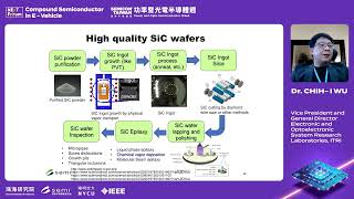
In compound semiconductor fabrication, choosing the right substrate is crucial for optimizing device performance. Common substrates include GaAs, InP, SiC, Sapphire, and Silicon, each tailored for specific applications. This section highlights the significance of lattice matching to minimize defects and dislocations that arise from lattice mismatch. Buffer and graded layers are often employed to manage strain and enhance film quality. The key substrates and their applications are summarized as follows:
- GaAs: Suited for AlGaAs and InGaAs in lasers and solar cells.
- InP: Ideal for InGaAsP and InGaAs in optical communication based applications.
- SiC: Utilized for GaN in high-power, RF, and LED devices.
- Sapphire: Best for cost-effective GaN blue LEDs.
Understanding substrate properties and suitable matching solutions is essential for producing efficient and reliable semiconductor devices.
Youtube Videos


Audio Book
Dive deep into the subject with an immersive audiobook experience.
Common Substrates
Chapter 1 of 3
🔒 Unlock Audio Chapter
Sign up and enroll to access the full audio experience
Chapter Content
- GaAs (for AlGaAs, InGaAs)
- InP (for InGaAsP, InGaAs)
- SiC (for GaN)
- Sapphire (for GaN)
- Silicon (heterogeneous integration)
Detailed Explanation
In compound semiconductor fabrication, the choice of substrate is crucial. Substrates are the foundational materials upon which semiconductor layers are built. Each substrate is selected based on its compatibility with the material being used. For instance, Gallium Arsenide (GaAs) substrates are often chosen for Aluminum Gallium Arsenide (AlGaAs) and Indium Gallium Arsenide (InGaAs) due to their similar lattice structures. Likewise, Indium Phosphide (InP) is preferred for applications involving InGaAsP and InGaAs. Silicon Carbide (SiC) and Sapphire substrates are typically used for Gallium Nitride (GaN) applications, including power and LED devices. For heterogeneous integration, silicon itself is used, allowing the combination of different types of semiconductors in a single device.
Examples & Analogies
Think of a construction project where you need a solid foundation to build a house. If you want to build a particularly tall building (like a powerful laser), you need a foundation that can support it. Each choice of substrate is similar to selecting the right foundation type, ensuring that the rest of the building (or semiconductor layers) can be built effectively without issues like sagging or cracking.
Lattice Mismatch Issue
Chapter 2 of 3
🔒 Unlock Audio Chapter
Sign up and enroll to access the full audio experience
Chapter Content
- Lattice mismatch can cause dislocations and defects
- Buffer layers and graded layers are used to minimize strain
Detailed Explanation
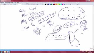
Lattice mismatch occurs when the lattice structure of the substrate does not align perfectly with that of the semiconductor material being deposited on it. This misalignment can lead to dislocations and defects in the crystal structure, which can severely affect the performance of semiconductor devices. To mitigate this issue, engineers use buffer layers—thin layers that smooth out the interface between the substrate and the semiconductor. Graded layers are also employed, where the composition gradually changes from that of the substrate to the semiconductor, reducing strain and helping to achieve better crystal quality.
Examples & Analogies
Imagine trying to fit two puzzle pieces that are slightly different shapes. If you force them together, they won't connect properly, leading to a poor picture. Instead, if you use a piece that has softer edges (like a buffer layer), it might help both pieces fit together more smoothly, producing a clearer image in the end (or in the case of semiconductors, a flawless electronic device).
Substrate Matched Materials Applications
Chapter 3 of 3
🔒 Unlock Audio Chapter
Sign up and enroll to access the full audio experience
Chapter Content
| Substrate | Matched Materials | Applications |
|---|---|---|
| GaAs | AlGaAs, InGaAs | Lasers, solar cells |
| InP | InGaAsP, InAlAs | Optical communication |
| SiC | GaN | High-power, RF, LEDs |
| Sapphire | GaN | Cost-effective blue LEDs |
Detailed Explanation
Different substrates support various materials which are optimized for particular applications. For instance, GaAs substrates are associated with AlGaAs and InGaAs, commonly used in lasers and solar cells due to their efficiency in converting light into electricity. InP substrates serve applications in optical communication, enabling high-speed data transfer. SiC is crucial for high-power and RF applications where heat resistance is important, while Sapphire is often chosen for GaN devices, especially in producing cost-effective blue LEDs. The choice of substrate directly impacts the performance and suitability of the semiconductor devices used in different technologies.
Examples & Analogies
Just as an athlete chooses the appropriate shoes for a specific sport (like running shoes for track vs. cleats for soccer), engineers select the right substrate for their semiconductor materials based on the application's requirements. Using the wrong substrate would be like wearing cleats on a running track - it won't perform as well.
Key Concepts
-
Substrate Selection: The choice of substrate directly affects the semiconductor device's efficiency and applicability.
-
Lattice Mismatch: Mismatch between substrate and film can lead to defects, impacting performance.
-
Buffer Layers: Used to reduce strain and defects due to lattice mismatches.
-
Applications: Different substrates are suited for various semiconductor applications based on their properties.
Examples & Applications
GaAs substrates are commonly used for fabricating laser diodes due to their excellent optical properties.
InP substrates are preferred in optical communication industries for devices like photonic integrated circuits.
Memory Aids
Interactive tools to help you remember key concepts
Rhymes
In the name of GaAs, layers grow fast, lattice match fine, our quality will last.
Stories
Imagine a chef carefully layering ingredients to create the perfect cake—just like substrates layer by layer ensure the best semiconductor devices.
Memory Tools
Remember: 'B-G-L' for choosing substrates: Buffer, GaAs, Lattice match.
Acronyms
SILG - Silicon, InP, Lattice considerations, GaAs.
Flash Cards
Glossary
- Substrate
The underlying material upon which a thin film is deposited during semiconductor fabrication.
- Lattice Mismatch
A condition that arises when the lattice constants of two different materials differ, leading to defects in thin film growth.
- Buffer Layer
A layer of material deposited between the substrate and the growing layer to reduce lattice mismatch effects.
- Graded Layer
A layer whose composition varies gradually to accommodate differences in lattice constants.
Reference links
Supplementary resources to enhance your learning experience.
