
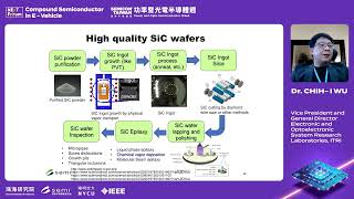
Key Epitaxial Growth Techniques
Interactive Audio Lesson
Listen to a student-teacher conversation explaining the topic in a relatable way.
Introduction to Epitaxial Growth Techniques
🔒 Unlock Audio Lesson
Sign up and enroll to listen to this audio lesson

Today, we will explore the essential epitaxial growth techniques for compound semiconductors. Can anyone tell me what epitaxy means?

I think it has to do with growing layers on top of a substrate.
Correct! Epitaxy involves depositing thin layers on a substrate, allowing precise control over material properties. Let's discuss MOCVD first. Who knows how it works?

Is it the one that uses metal-organic precursors?
Exactly! MOCVD uses metal-organic precursors, like Trimethylgallium, which decompose at high temperatures. Remember, MOCVD stands for Metal-Organic Chemical Vapor Deposition. A mnemonic could be 'Mighty Organics Create Delicate Vapor'. Now, could someone explain its advantages?

It has high throughput and can control compositions well.
Great job! Its high throughput is particularly beneficial for mass production of devices like LEDs. However, what is a limitation of MOCVD?

It requires high temperatures, right?
That's right! Temperatures can reach between 600 to 1100 degrees Celsius. Let's move on to MBE.
Molecular Beam Epitaxy (MBE)
🔒 Unlock Audio Lesson
Sign up and enroll to listen to this audio lesson

MBE stands for Molecular Beam Epitaxy. Can anyone share how MBE differs from MOCVD?
It uses ultra-high vacuum for evaporating elemental sources.
Exactly! MBE requires an ultra-high vacuum environment which allows for atomic-level precision. A mnemonic for MBE might be 'Molecular Beams Elegantly'. What are some materials we can grow using MBE?
GaAs and InP, right?
Great memory! MBE is excellent for research but what do we need to keep in mind about its limitations?
It's more expensive and has low throughput compared to MOCVD?
Spot on! The expense and complexity are significant aspects. Let's wrap this session up. Can anyone summarize the key points about MBE?
MBE uses ultra-high vacuum for precision, supports materials like GaAs, and has higher costs.
Hydride Vapor Phase Epitaxy (HVPE)
🔒 Unlock Audio Lesson
Sign up and enroll to listen to this audio lesson
Now let's discuss HVPE. What does it primarily grow?
GaN for bulk substrates!
Correct! HVPE grows thick layers of GaN. Can someone recall its working principle?
It uses reactions of hydrogen halides with metal sources.
Exactly! However, what is a notable limitation of HVPE?
It has less control over thin film composition.
That's right! This technique is primarily used for substrate production. Remember, HVPE's strengths are in high-quality substrate production but with limitations in film control.
Liquid Phase Epitaxy (LPE)
🔒 Unlock Audio Lesson
Sign up and enroll to listen to this audio lesson
Let's finish with LPE. Can anyone explain how LPE works?
Material is grown from a supersaturated liquid solution?
Exactly! LPE, or Liquid Phase Epitaxy, is used less frequently now. What kind of devices did it primarily support?
Older generation GaAs lasers and basic optical devices.
Correct! However, why has LPE been largely replaced?
Because of its poor precision compared to other methods?
Well said! To summarize today, we explored the four main epitaxial techniques: MOCVD, MBE, HVPE, and LPE, highlighting their advantages, limitations, and applications.
Introduction & Overview
Read summaries of the section's main ideas at different levels of detail.
Quick Overview
Standard
The section outlines essential epitaxial growth techniques for compound semiconductors, detailing their working principles, advantages, limitations, and suitable materials. Techniques like MOCVD and MBE are highlighted for their applications in advanced electronic and optoelectronic devices.
Detailed
Key Epitaxial Growth Techniques
Epitaxial growth techniques are crucial for the fabrication of compound semiconductors, enabling precise control over layer properties and achieving optimal device performance. Here are the key techniques discussed:
- MOCVD (Metal-Organic Chemical Vapor Deposition):
- Working Principle: Utilizes metal-organic precursors decomposed at high temperatures in a reactor, allowing thin films to grow on heated substrates via surface reactions.
- Supported Materials: GaAs, GaN, InP, AlGaAs, InGaN.
- Advantages: Offers high throughput, precise compositional control, and is suitable for mass production of LEDs and laser diodes.
- Limitations: Requires high temperatures (600–1100°C) and handles toxic gases.
- MBE (Molecular Beam Epitaxy):
- Working Principle: Employs ultra-pure elemental sources evaporated in ultra-high vacuum (UHV), allowing atoms to condense on a cooled substrate.
- Supported Materials: GaAs, InP, InGaAs, AlGaAs, HgCdTe.
- Advantages: Achieves atomic-level precision and is excellent for research purposes.
- Limitations: Low throughput and high complexity due to UHV requirements.
- HVPE (Hydride Vapor Phase Epitaxy):
- Working Principle: Involves reactions of hydrogen halides with metal sources for growing thick layers.
- Supported Materials: Primarily GaN for bulk substrate growth.
- Applications: Useful for producing high-quality GaN substrates for blue LEDs and high-power devices.
- Limitations: Less control over thin film composition compared to MOCVD and MBE.
- LPE (Liquid Phase Epitaxy):
- Working Principle: Material is grown from a supersaturated solution in a liquid state.
- Applications: Used in basic optical devices and older generation lasers.
- Limitations: Offers poor precision and has been largely replaced by MOCVD and MBE in modern applications.
In summary, understanding these techniques is vital in the advancement of semiconductor technologies, especially in optoelectronic applications.
Youtube Videos
Audio Book
Dive deep into the subject with an immersive audiobook experience.
MOCVD (Metal-Organic Chemical Vapor Deposition)
Chapter 1 of 6
🔒 Unlock Audio Chapter
Sign up and enroll to access the full audio experience
Chapter Content
MOCVD (Metal-Organic Chemical Vapor Deposition)
- Working Principle:
Metal-organic precursors (e.g., Trimethylgallium, Arsine) are decomposed at high temperature in a reactor.
Thin films grow via surface chemical reactions on heated substrates. - Materials Supported: GaAs, GaN, InP, AlGaAs, InGaN
- Advantages:
- High throughput (scalable for mass production)
- Precise control over composition (suitable for ternary/quaternary alloys)
- Ideal for LEDs, laser diodes, and HEMTs
- Limitations:
- High temperature (~600–1100°C)
- Toxic and pyrophoric gases
Detailed Explanation
MOCVD is a widely used technique for growing thin films of semiconductors. It operates by introducing metal-organic compounds into a reactor at high temperatures. Here, the precursors decompose chemically to create thin layers on the substrate. This method excels at producing high-quality materials, particularly for devices like LEDs and laser diodes, due to its high throughput and precision in the composition of materials.
Examples & Analogies
Think of MOCVD like baking a cake in which you carefully add specific ingredients to create a perfect recipe. Just as a baker controls temperature and ingredient types, engineers control the reaction conditions and compounds used to ensure they achieve the best material properties for their devices.
Advantages and Limitations of MOCVD
Chapter 2 of 6
🔒 Unlock Audio Chapter
Sign up and enroll to access the full audio experience
Chapter Content
- Advantages:
- High throughput (scalable for mass production)
- Precise control over composition (suitable for ternary/quaternary alloys)
- Ideal for LEDs, laser diodes, and HEMTs
- Limitations:
- High temperature (~600–1100°C)
- Toxic and pyrophoric gases
Detailed Explanation
MOCVD's primary advantages lie in its ability to produce large quantities of semiconductor material efficiently while maintaining precise control over the composition of those materials. However, the process has limitations, including requiring high temperatures, which can complicate the manufacturing process and introduce safety concerns due to the use of toxic gases.
Examples & Analogies
Imagine a factory that can consistently produce high-quality products quickly. However, the factory's operation needs to be cautious because it involves dangerous materials. Similarly, MOCVD provides efficient production but requires careful handling of high temperatures and toxic chemicals.
MBE (Molecular Beam Epitaxy)
Chapter 3 of 6
🔒 Unlock Audio Chapter
Sign up and enroll to access the full audio experience
Chapter Content
MBE (Molecular Beam Epitaxy)
- Working Principle:
Ultra-pure elemental sources are evaporated under ultra-high vacuum (UHV).
Atoms condense on the cooled substrate to form epitaxial layers. - Materials Supported: GaAs, InP, InGaAs, AlGaAs, HgCdTe
- Advantages:
- Atomic-level precision and abrupt interfaces
- Excellent for research and prototyping
- Lower growth temperature than MOCVD
- Limitations:
- Low throughput
- High cost and complexity
- Requires ultra-high vacuum (~10⁻⁹ Torr)
Detailed Explanation
MBE is a technique that achieves extremely thin and precise layers of material through the evaporation of atoms and their condensation on cooler substrates in a vacuum environment. It is ideal for research and developing advanced devices due to its precision but is limited by its slower production rates and higher costs.
Examples & Analogies
Imagine sculpting a statue out of marble with utmost care, where each touch must be precise and purposeful. MBE works similarly; it builds up materials with such precision that you can control the atomic-level properties of the final product.
Advantages and Limitations of MBE
Chapter 4 of 6
🔒 Unlock Audio Chapter
Sign up and enroll to access the full audio experience
Chapter Content
- Advantages:
- Atomic-level precision and abrupt interfaces
- Excellent for research and prototyping
- Lower growth temperature than MOCVD
- Limitations:
- Low throughput
- High cost and complexity
- Requires ultra-high vacuum (~10⁻⁹ Torr)
Detailed Explanation
While MBE offers unmatched precision, making it perfect for advanced research applications, it struggles with throughput, as producing a layer takes significantly longer compared to MOCVD. Additionally, the high operational costs and the necessity for an ultra-high vacuum environment can limit its widespread use in commercial applications.
Examples & Analogies
Think of MBE like a high-end tailored suit. It takes more time and effort to produce a suit that fits perfectly, making it a premium option rather than a mass-market product like ready-to-wear clothing, which can be produced much more quickly and cheaply.
HVPE (Hydride Vapor Phase Epitaxy)
Chapter 5 of 6
🔒 Unlock Audio Chapter
Sign up and enroll to access the full audio experience
Chapter Content
HVPE (Hydride Vapor Phase Epitaxy)
- Working Principle:
Uses reactions of hydrogen halides (like HCl) with metal sources to grow thick layers - Materials Supported: GaN (bulk substrate growth)
- Applications:
- High-quality GaN substrates for blue LEDs and high-power GaN devices
- Limitations:
- Less control over thin film composition
- Mostly used for substrate production
Detailed Explanation
HVPE is primarily used to grow thick layers of GaN by using chemical reactions in the vapor phase. It is particularly valued for producing bulk substrates needed in high-performance devices like blue LEDs. However, its drawback is the reduced ability to control the detailed composition of thin films.
Examples & Analogies
Imagine a conveyor belt producing large sheets of metal. While you can create a lot of material quickly, you may not be able to control every detail of its composition. HVPE operates similarly: it’s efficient for creating substantial layers but lacks the fine control of other methods.
LPE (Liquid Phase Epitaxy)
Chapter 6 of 6
🔒 Unlock Audio Chapter
Sign up and enroll to access the full audio experience
Chapter Content
LPE (Liquid Phase Epitaxy)
- Working Principle:
Material is grown from a supersaturated solution in a liquid melt - Applications:
Basic optical devices, older generation of GaAs lasers - Limitations:
Poor precision, replaced by MOCVD/MBE in modern devices
Detailed Explanation
LPE allows the growth of semiconductor materials from a liquid phase, similar to making candy by boiling sugar and then letting it cool. However, this technique has been largely replaced by more precise methods like MOCVD and MBE because it lacks the accuracy required for contemporary applications.
Examples & Analogies
Think of LPE as making homemade jelly on a stovetop. While it can create a product, the outcome can vary greatly depending on how you control the heat and ingredients, making it less reliable than using a professionally made fruit spread, just as MOCVD and MBE provide more reliably precise results.
Key Concepts
-
MOCVD: A growth method using metal-organic precursors under chemical vapor conditions with high throughput.
-
MBE: A delicate process that allows atomic precision in layer deposition under ultra-high vacuum conditions.
-
HVPE: A thick layer growth method suitable for bulk substrates, mainly GaN.
-
LPE: A traditional method for growing optical devices but less precise than modern alternatives.
Examples & Applications
MOCVD is commonly used to produce layers of GaN for blue LEDs.
MBE is utilized in the fabrication of atomic-scale structures for quantum devices.
Memory Aids
Interactive tools to help you remember key concepts
Rhymes
MOCVD's great for layers that are neat; high temps are required, but production's a treat.
Stories
Once there was a chemist named Moby, who loved his clean labs for MBE. In his vacuum realm, he crafted with care, layers so precise, it was quite rare!
Memory Tools
For MOCVD, think 'Metal Organics Create Very Delicate' layers.
Acronyms
MBE - 'Molecular Beams Elegantly' deposits atomic layers.
Flash Cards
Glossary
- Epitaxy
The deposition of layers of crystalline material on a crystalline substrate.
- MOCVD
Metal-Organic Chemical Vapor Deposition, a method for growing thin films through chemical reactions of metal-organic precursors.
- MBE
Molecular Beam Epitaxy, a technique using thermal evaporation in a highly controlled vacuum environment.
- HVPE
Hydride Vapor Phase Epitaxy, a method utilizing hydrogen halides to grow thick crystalline layers.
- LPE
Liquid Phase Epitaxy, a growth method involving the deposition from a supersaturated solution.
Reference links
Supplementary resources to enhance your learning experience.