
Problem Statement
Interactive Audio Lesson
Listen to a student-teacher conversation explaining the topic in a relatable way.
The Inadequacy of Silicon Methods
🔒 Unlock Audio Lesson
Sign up and enroll to listen to this audio lesson

Let's start by discussing why traditional silicon fabrication can't be fully applied to compound semiconductors. Can anyone guess what key factors differ between silicon and compound semiconductors?

Is it because of their different atomic structures?
Exactly! The atomic composition and crystal structures are different, which means that their properties often lead to issues if traditional silicon methods are used. They might not achieve the necessary electrical characteristics.

What kinds of properties are we talking about?
Great question! We're mainly concerned with electrical and optical properties, which include how well they can conduct electricity or emit light, depending on their applications.

So, what does that mean for our fabrication techniques?
It means we need to turn to specialized methods. This leads us to epitaxial techniques, which we will discuss shortly. But let's summarize: traditional silicon techniques face significant limitations due to the unique properties of compound semiconductors, particularly in achieving desired electrical characteristics.
Epitaxial Techniques
🔒 Unlock Audio Lesson
Sign up and enroll to listen to this audio lesson

Now, let's talk about how epitaxial techniques address these challenges. Can anyone tell me what MOCVD stands for?

It stands for Metal-Organic Chemical Vapor Deposition!
Correct! MOCVD is crucial for growing thin films precisely. What about MBE?
Molecular Beam Epitaxy?
Exactly! MBE allows atomic-level precision in layer formation, making them invaluable for our applications. But what challenges do you think we might face when growing high-quality films?
Maybe controlling the temperature? I’ve heard that’s important.
Right again! Temperature control is critical, especially since the quality of the films can significantly affect device performance. Any other challenges?
I guess dealing with mismatched materials could also be an issue?
You're spot on! Mismatched lattice structures can lead to defects. Remember, achieving high-quality films is essential for device success. Summarizing: MOCVD and MBE are vital techniques, yet they come with challenges, including temperature control and material matching.
The Importance of High-Quality Films
🔒 Unlock Audio Lesson
Sign up and enroll to listen to this audio lesson
Let's dive deeper into why high-quality films are important. What happens if the films aren't of high quality?
Would the devices not work as expected?
Exactly! If the films have defects or irregularities, it can severely hinder the device's efficiency. They might not even work right at all.
So, high-quality material is key to performance?
Absolutely! You need that layer quality to ensure optimal charge transport and light emission in optoelectronic devices. Can anyone think of examples where this is particularly important?
Like in LEDs or laser diodes?
Exactly! In these applications, even small defects can lead to major performance drops. To summarize, high-quality film growth is vital for the functional and reliable operation of semiconductor devices.
Introduction & Overview
Read summaries of the section's main ideas at different levels of detail.
Quick Overview
Standard
Traditional silicon fabrication methods fail to address the unique properties of compound semiconductors, requiring specialized techniques like molecular beam epitaxy (MBE) and metal-organic chemical vapor deposition (MOCVD) for optimal device performance. This section also explores the challenges associated with the growth of high-quality compound semiconductor films.
Detailed
Problem Statement
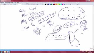
Fabricating compound semiconductors presents unique challenges not addressed by traditional silicon techniques. The critical differences include the need for precise control over composition, crystalline quality, and layer thickness, which are vital for achieving specific electrical and optical properties. This section poses fundamental questions: Why can't conventional silicon processes be applied to compound semiconductors? The variations in bandgap, lattice structures, and chemical behavior of the materials necessitate specialized methods.
Epitaxial techniques such as MOCVD and MBE provide the required precision and are essential in the development of high-performance optoelectronic and electronic devices. However, these methods come with their own set of challenges, particularly in maintaining the quality of the grown films, which is paramount for the devices' efficiency and scalability. This section serves as an introduction to understanding the complex landscape of compound semiconductor fabrication.
Youtube Videos
Audio Book
Dive deep into the subject with an immersive audiobook experience.
Traditional Silicon Fabrication Limitations
Chapter 1 of 3
🔒 Unlock Audio Chapter
Sign up and enroll to access the full audio experience
Chapter Content
Why can’t traditional silicon fabrication methods be fully applied to compound semiconductors?
Detailed Explanation
Traditional silicon fabrication is designed around the properties of silicon, which differs significantly from compound semiconductors. Silicon has a stable crystal structure and electrical properties that align well with existing production methods. Compound semiconductors, like GaAs or InP, possess a different atomic arrangement and electronic behavior that requires specific conditions for growth and processing. This limitation means that techniques effective in silicon may not yield high-quality results or reliable performance with compound semiconductors.
Examples & Analogies
Think of traditional silicon like a standard recipe for making bread. If you try to use that same recipe to make a cake, you might find that the cake doesn’t rise properly because the ingredients and techniques suitable for bread don’t work for cake. Similarly, the inherent properties of silicon don’t translate well to compound semiconductors.
Role of Epitaxial Techniques
Chapter 2 of 3
🔒 Unlock Audio Chapter
Sign up and enroll to access the full audio experience
Chapter Content
How do epitaxial techniques like MOCVD and MBE enable high-performance optoelectronic and electronic devices?
Detailed Explanation
Epitaxial techniques such as Metal-Organic Chemical Vapor Deposition (MOCVD) and Molecular Beam Epitaxy (MBE) allow for the precise growth of compound semiconductor layers. These methods enable engineers to control layer thickness, composition, and the quality of the crystal structure, all of which are critical for the devices’ performance. MOCVD, for instance, uses gaseous reactants to deposit layers at relatively high temperatures, while MBE uses beams of atoms in a vacuum to achieve atomic-level precision. This meticulous control translates to better electronic and optoelectronic properties, crucial for applications like lasers and high-efficiency solar cells.
Examples & Analogies
Imagine building a multi-layered cake where each layer must be perfectly aligned and exactly the right thickness. If you were to sloppily add layers, the structure would collapse and the flavors might clash. Epitaxial growth is like the careful process of layering that cake, ensuring each layer complements the others and results in a seamless, high-quality final product.
Challenges in Growing High-Quality Films
Chapter 3 of 3
🔒 Unlock Audio Chapter
Sign up and enroll to access the full audio experience
Chapter Content
What challenges arise in growing high-quality compound semiconductor films?
Detailed Explanation
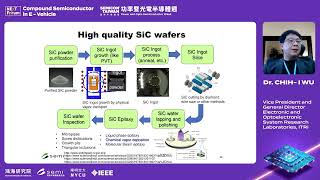
Growing high-quality compound semiconductor films presents several challenges. Firstly, achieving the right layer thickness and uniformity is crucial; too thick or insufficiently uniform films can lead to defects and degraded performance. Secondly, the lattice mismatch between the substrate and the deposited layer can introduce dislocations, leading to material defects. Additionally, controlling impurity levels is vital as contaminants can greatly affect the electrical properties of the final device. These challenges require specialized techniques and conditions to ensure high-quality material is produced.
Examples & Analogies
Think of it like trying to paint a delicate canvas. If the paint is too thick, it can run and ruin the artwork; if there are dust or impurities on the canvas, they can spoil the finish. Similarly, in semiconductor manufacturing, achieving the right conditions and cleanliness is vital to producing a flawless product.
Key Concepts
-
Epitaxial Growth: A critical method for the fabrication of high-quality compound semiconductor films.
-
Silicon Limitations: Traditional silicon fabrication techniques do not adequately address the distinct processes needed for compound semiconductors.
-
Defect-Compromised Performance: High-quality film growth significantly impacts device performance and efficiency.
Examples & Applications
MOCVD is often used to fabricate thin layers of Gallium Nitride (GaN) for blue LEDs, capitalizing on its precise control over layer composition.
MBE is favored for research and prototyping due to its atomic-level precision, especially critical in developing high-performance laser diodes.
Memory Aids
Interactive tools to help you remember key concepts
Rhymes
In MBE, atoms flow, on the substrate they glow, for precision so bright, making devices a delight.
Stories
Imagine a chef trying to bake a perfect cake. If they use the wrong temperatures and ingredients, the cake won’t rise. Similarly, using the wrong techniques for some semiconductors can lead to failures in performance.
Memory Tools
Remember 'MOCVD' with 'Most Optimal Compound Vapor Delivery.' It highlights how this method ensures the best delivery of material properties.
Acronyms
To remember MBE, think 'Molecular Beam Excellence' – emphasizing its precision in semiconductor fabrication.
Flash Cards
Glossary
- Epitaxy
A method used to grow thin films of crystalline materials on a substrate.
- MOCVD
Metal-Organic Chemical Vapor Deposition, a technique used for growing thin films with precise composition control.
- MBE
Molecular Beam Epitaxy, a method for growing high-purity layers with atomic-level control.
- Lattice Mismatch
A condition where the atomic spacing of two different materials does not align, potentially causing defects.
- Optoelectronic Devices
Devices that detect or control light as well as electrical signals, such as LEDs and laser diodes.
Reference links
Supplementary resources to enhance your learning experience.