
Conclusion
Interactive Audio Lesson
Listen to a student-teacher conversation explaining the topic in a relatable way.
Importance of Epitaxial Growth Techniques
🔒 Unlock Audio Lesson
Sign up and enroll to listen to this audio lesson

Students, today we're wrapping up our exploration of compound semiconductors! Let's start by discussing why epitaxial growth techniques like MOCVD and MBE are essential for device performance. Why do you think these techniques are so impactful?

I think it's because they allow for very precise control over the material properties, which is crucial for making advanced devices.
Exactly! That precision is vital for achieving the desired electrical and optical properties. This leads us to high-performance devices. Can anyone give examples of such devices?

LEDs and laser diodes are examples, right?
Yes, those are perfect examples! Now, let’s summarize: the quality of the epitaxial layers directly influences overall device effectiveness.
Advancements in Compound Semiconductor Fabrication
🔒 Unlock Audio Lesson
Sign up and enroll to listen to this audio lesson

In this session, we will discuss how advancements in adaptation techniques affect fabrication. Can anyone tell me the relevance of scalable production?

Scalable production means we can produce more devices cost-effectively and meet increased demand.
Exactly! This is crucial for the widespread adoption of these technologies. How do you think we can integrate these devices into everyday applications?

By using them in telecom and power sectors! Like improving our mobile connections!
Right! Innovations in heterogeneous integration also aid in this process.
Future Directions in Compound Semiconductor Technology
🔒 Unlock Audio Lesson
Sign up and enroll to listen to this audio lesson
In the last part, let's think about the future of compound semiconductors. What do you imagine will be the key trends based on what we've learned?
I think the focus will shift towards making devices even more efficient and environmentally friendly.
Great point! Sustainability and efficiency are essential in the tech world. How can advancements in epitaxial growth help us achieve that?
If we refine the techniques further, we could reduce waste and create devices that consume less power.
Absolutely! Continuous improvement in these areas will lead to the greater adoption of compound semiconductors.
Introduction & Overview
Read summaries of the section's main ideas at different levels of detail.
Quick Overview
Standard
This section concludes that the development of techniques like MOCVD and MBE plays a pivotal role in achieving the necessary control over the properties of compound semiconductors. These advancements are crucial for scaling production and promoting their adoption in various high-tech applications such as telecom and photonics.
Detailed
Conclusion
The performance of compound semiconductor devices relies heavily on the quality of the epitaxial layers produced during fabrication. High-precision techniques like Metal-Organic Chemical Vapor Deposition (MOCVD) and Molecular Beam Epitaxy (MBE) provide the atomic-level control necessary for crafting highly efficient optoelectronic and electronic components. The advancements in epitaxial growth methods, alongside innovations in heterogeneous integration, suggest that the fabrication of compound semiconductors is moving towards greater scalability. This positions compound semiconductors for broader applications, including in telecommunications, power management, and photonics sectors.
Youtube Videos

Audio Book
Dive deep into the subject with an immersive audiobook experience.
Importance of High-Quality Epitaxial Layer Growth
Chapter 1 of 4
🔒 Unlock Audio Chapter
Sign up and enroll to access the full audio experience
Chapter Content
The performance of compound semiconductor devices begins with high-quality epitaxial layer growth.
Detailed Explanation
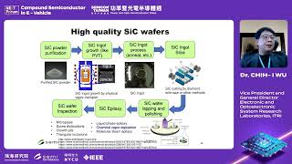
The performance of devices made from compound semiconductors heavily relies on the quality of the layers grown during fabrication. Epitaxial growth is a method where layers of semiconductor material are deposited on a substrate in a highly controlled manner. When these layers are of high quality, the resulting devices perform better, allowing for greater efficiency and speed in optoelectronic applications.
Examples & Analogies
Consider building a multi-story building; the quality of the foundation and the materials used to build each floor impacts the overall stability and functionality of the structure. Similarly, in semiconductor manufacturing, high-quality layers support better device performance.
Techniques for Layer Growth
Chapter 2 of 4
🔒 Unlock Audio Chapter
Sign up and enroll to access the full audio experience
Chapter Content
Techniques like MOCVD and MBE offer the atomic-level control needed for high-speed and optoelectronic devices.
Detailed Explanation
MOCVD (Metal-Organic Chemical Vapor Deposition) and MBE (Molecular Beam Epitaxy) are two prominent methods used to achieve the precise atomic-level control necessary for creating effective compound semiconductor devices. MOCVD allows for mass production while MBE is well-suited for research environments due to its precision. This level of control is crucial for fabricating devices like LEDs and laser diodes, which have specific performance requirements.
Examples & Analogies
Think of these techniques as cooking methods. MOCVD is like a large kitchen where many chefs can prepare several dishes at once (suitable for production), while MBE is like a fine-dining kitchen with one chef meticulously crafting a single exquisite dish (great for research). Both methods require skill and precision, but they serve different purposes.
Advancements in Compound Semiconductor Fabrication
Chapter 3 of 4
🔒 Unlock Audio Chapter
Sign up and enroll to access the full audio experience
Chapter Content
With advancements in growth methods and heterogeneous integration, compound semiconductor fabrication is becoming more scalable.
Detailed Explanation
Recent developments in the field of semiconductor fabrication are focusing on improving scaling techniques, which allows for mass production of compound semiconductors. By integrating different materials (heterogeneous integration), manufacturers can enhance device capabilities and expand their applications across various industries, such as telecommunications and power electronics.
Examples & Analogies
Envision a city that evolves to accommodate more people by building higher skyscrapers and connecting different neighborhoods with efficient transport systems. Similarly, advancements in semiconductor fab techniques allow the 'city' of electronic devices to grow and improve, meeting the demands of modern technology.
Diverse Applications of Compound Semiconductors
Chapter 4 of 4
🔒 Unlock Audio Chapter
Sign up and enroll to access the full audio experience
Chapter Content
This is paving the way for their widespread adoption across telecom, power, and photonics sectors.
Detailed Explanation
The improvement and scalability of compound semiconductor fabrication have resulted in their increased use in various fields such as telecommunications, power systems, and photonics. These sectors rely on the advanced properties of compound semiconductors for developing high-performance electronic devices, such as smartphones, LED lighting, and solar panels.
Examples & Analogies
Just as companies like Apple or Samsung continuously innovate and implement advanced technologies into their products, the adoption of compound semiconductors is transforming industries by enabling the development of cutting-edge devices that we use in our daily lives.
Key Concepts
-
Epitaxial Layer Quality: Influences device performance directly.
-
MOCVD and MBE: Key techniques providing atomic-level control.
-
Scalability: Essential for widespread adoption in various sectors.
Examples & Applications
The development of high-speed optical communication devices.
The use of compound semiconductors in high-efficiency solar cells.
Memory Aids
Interactive tools to help you remember key concepts
Rhymes
In a cleanroom we grow, layer by layer, for devices that glow, making tech even greater.
Stories
Imagine a chef layering ingredients just right to bake a perfect cake. Epitaxial growth is like that—each layer must be correct to ensure the final semiconductor device works perfectly.
Memory Tools
Remember 'MEG', M for MOCVD, E for Epitaxial quality, and G for Growth importance.
Acronyms
Use 'REAL' - R for Reliability, E for Efficiency, A for Applications, L for Layer quality.
Flash Cards
Glossary
- Epitaxial Growth
A method of depositing thin crystalline films on a substrate to control the thickness and properties of layers.
- MOCVD
Metal-Organic Chemical Vapor Deposition, a technique used to grow thin films of semiconductors.
- MBE
Molecular Beam Epitaxy, a technique for growing highly controlled thin films in a vacuum environment.
- Scalability
The ability to increase production volume without a significant increase in costs.
Reference links
Supplementary resources to enhance your learning experience.