Introduction
Interactive Audio Lesson
Listen to a student-teacher conversation explaining the topic in a relatable way.
Importance of Precision in Fabrication
🔒 Unlock Audio Lesson
Sign up and enroll to listen to this audio lesson

Today, we're introducing the significance of precision in the fabrication of compound semiconductors. Why do you think being precise with atomic composition and layer thickness matters?

I think it might affect how well the semiconductor can conduct electricity.

Exactly, that electrical conductivity plays a major role in device performance. If the atomic composition is off, it can lead to defects. Now, can someone explain what epitaxial techniques are?

Epitaxial techniques involve growing layers on a substrate to tailor the material's properties.

Right! This method allows for precise control of material properties, unlike traditional silicon-based methods. Remember the acronym 'PEEL': Precise Epitaxial Engineering Layers.

What happens if the layer thickness is incorrect?

Good question! Incorrect thickness can lead to suboptimal performance, such as reduced efficiency. In summary, precision in semiconductor fabrication is vital for enhancing electrical and optical functionalities, laying the groundwork for advanced technologies.
Comparison to Silicon
🔒 Unlock Audio Lesson
Sign up and enroll to listen to this audio lesson

Let's delve into why traditional silicon fabrication techniques can't be fully applied to compound semiconductors. Student_4, do you know any differences?

Silicon has a more straightforward fabrication process, right?

Yes, silicon is a mature technology with established methods. Compound semiconductors, however, require more tailored approaches like epitaxy to exploit their unique properties. Who can give me an example of a compound semiconductor?

Maybe gallium arsenide - GaAs?

Exactly! GaAs is widely used in optoelectronics. Remember the mnemonic 'GOAT': Gallium, Optoelectronics, Arsenide Technology. Summarizing, while silicon is simpler, compound semiconductors offer specific advantages that require intricate fabrication techniques.
Epitaxial Growth Techniques
🔒 Unlock Audio Lesson
Sign up and enroll to listen to this audio lesson

Now, let’s explore the core topic: epitaxial growth techniques for these semiconductors. Can anyone describe what we mean by 'epitaxial growth'?

It’s when layers are deposited on a substrate to create a specific crystal structure.

Exactly! And this layer-by-layer approach allows for precision. Let's use 'SMART'—Structured Material Advance via Radical Technique—as a memory aid for remembering how this enables better control over properties. Why do you think this is advantageous for modern devices?

It allows us to create devices that operate efficiently with tailored properties.

Correct! Tailoring properties leads to better device performance. In conclusion, understanding these techniques is crucial as they form the basis for the subsequent chapters where we delve deeper into the fabrication processes.
Introduction & Overview
Read summaries of the section's main ideas at different levels of detail.
Quick Overview
Standard
This introduction details the critical importance of precise control over atomic composition, crystal quality, and layer thickness in the fabrication of compound semiconductors. It highlights the epitaxial growth techniques that allow for the tailoring of material properties essential for advanced devices compared to traditional silicon methods.
Detailed
Introduction to the Fabrication of Compound Semiconductors
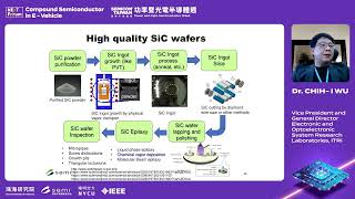
The fabrication of compound semiconductors involves meticulous control of factors such as atomic composition, crystal quality, and the thickness of layers. This precision is crucial for obtaining optimal electrical and optical properties necessary for modern high-performance devices. Unlike silicon, which has established fabrication practices, compound semiconductors often employ epitaxial techniques. This approach facilitates a layer-by-layer deposition on a substrate, allowing engineers to tailor material properties effectively.
In this section, we will introduce the primary fabrication methodologies used for compound semiconductors, focusing extensively on epitaxial growth techniques. We will also discuss the advantages, limitations, and various applications of these methods, setting the stage for deeper exploration of advanced materials.
Youtube Videos


Audio Book
Dive deep into the subject with an immersive audiobook experience.
Importance of Precision in Fabrication
Chapter 1 of 3
🔒 Unlock Audio Chapter
Sign up and enroll to access the full audio experience
Chapter Content
Fabricating compound semiconductors requires precise control over atomic composition, crystal quality, and layer thickness.
Detailed Explanation
The fabrication of compound semiconductors is a meticulous process that demands precision. This means that engineers must carefully manage several critical factors such as the atomic makeup of the materials, the quality of the crystal structures, and the thickness of the layers being created. Each of these elements is crucial, as they directly influence the final performance of the semiconductor device. Poor control of any of these factors can lead to devices that do not work correctly or efficiently.
Examples & Analogies
Think of fabricating semiconductors like baking a complex cake. Each ingredient (like the atomic composition) must be measured precisely, the mix (crystal quality) should blend well, and the baking time (layer thickness) must be just right. If one aspect is off, you might end up with a cake that's too dry or undercooked, just like a semiconductor device can fail if not fabricated correctly.
Epitaxial Techniques
Chapter 2 of 3
🔒 Unlock Audio Chapter
Sign up and enroll to access the full audio experience
Chapter Content
Unlike silicon, compound semiconductors are often grown using epitaxial techniques, which allow engineers to tailor material properties through layer-by-layer deposition on a substrate.
Detailed Explanation
Epitaxy is a process used to grow thin films of semiconductor materials on a substrate crystal. This method is particularly important for compound semiconductors because it offers the ability to build up layers with specific properties, enabling custom designs for better electrical and optical performance. Unlike traditional silicon materials, which can be more simplistic in their fabrication processes, compound semiconductors benefit significantly from this sophisticated approach.
Examples & Analogies
Imagine building a multi-layer cake where each layer has a different flavor and texture, carefully stacked to create a delightful final product. In semiconductor terms, each layer represents unique materials that enhance the overall properties of the device, much like how each cake layer contributes to the overall flavor.
Overview of Fabrication Methods
Chapter 3 of 3
🔒 Unlock Audio Chapter
Sign up and enroll to access the full audio experience
Chapter Content
This chapter introduces the core fabrication methods used for compound semiconductors, with an emphasis on epitaxial growth techniques, and discusses their advantages, limitations, and applications.
Detailed Explanation
This section provides an overview of the main methods utilized in the fabrication of compound semiconductors, particularly focusing on epitaxial growth techniques. It covers various aspects, including the benefits and drawbacks of each method, alongside their relevant uses in real-world applications. Understanding these methods is central to grasping how advanced compound semiconductor devices are manufactured.
Examples & Analogies
Consider this like a toolkit for a mechanic. Just as different tools are better for specific tasks, various fabrication methods are suited to different types of semiconductor devices. By learning about each tool's strengths and weaknesses, one can better understand how to fix or build sophisticated machines.
Key Concepts
-
Epitaxial Techniques: Methods that allow the layer-by-layer deposition of materials, tailoring their properties for advanced semiconductor applications.
-
Precision Control: The need for accurate control over atomic composition, crystal quality, and layer thickness to achieve optimized device performance.
Examples & Applications
Gallium Arsenide (GaAs) is commonly used in optoelectronics due to its effective light-emitting properties.
Indium Phosphide (InP) is pivotal in high-speed telecommunications.
Memory Aids
Interactive tools to help you remember key concepts
Rhymes
To grow those layers nice and thin, Epitaxial growth is where we begin!
Stories
Imagine a chef making a layered cake, each layer carefully measured for perfect taste—this is like epilayer growth in semiconductors!
Memory Tools
To recall the steps of epitaxy: Layers, Precision, Growth—'LPG' to remember!
Acronyms
PEEL
Precise Epitaxial Engineering Layers
way to remember the root of this technology.
Flash Cards
Glossary
- Compound Semiconductors
Materials composed of two or more elements which have semiconductor properties, often exhibiting superior performance in specific applications.
- Epitaxial Growth
A process where crystalline layers are deposited on a substrate, allowing tailored material properties essential for advanced semiconductor devices.
- Atomic Composition
The arrangement and types of atoms present in a material, affecting its electrical and optical characteristics.
- Crystal Quality
A measure of the structural integrity of a crystal, impacting its performance in semiconductor applications.
Reference links
Supplementary resources to enhance your learning experience.
