
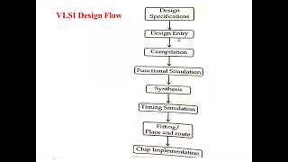
Cell Sizing and Resizing
Enroll to start learning
You’ve not yet enrolled in this course. Please enroll for free to listen to audio lessons, classroom podcasts and take practice test.
Interactive Audio Lesson
Listen to a student-teacher conversation explaining the topic in a relatable way.
Introduction to Cell Sizing
🔒 Unlock Audio Lesson
Sign up and enroll to listen to this audio lesson

Today, we will discuss cell sizing and how it influences the area and performance in VLSI design. Can anyone tell me what cell sizing means?

Is it about how large the logic gates are on the chip?
Exactly! Cell sizing refers to adjusting the size of logic cells—larger cells can improve performance, but they also increase the area. This leads to potential trade-offs, which we’ll explore.

So if I make all my cells smaller, I can save space, right?
Yes, but remember that smaller cells can affect speed. This is a classic example of optimization, where we must balance area and performance. A mnemonic to remember this is 'SAS'—'Space And Speed.'
Benefits and Trade-offs of Cell Resizing
🔒 Unlock Audio Lesson
Sign up and enroll to listen to this audio lesson

Now, let’s dive deeper into the benefits and trade-offs of resizing cells. Can anyone give me an example of how a trade-off might arise?

If I resize my cells to be smaller, I save area, but they might not work as fast?
Exactly, great point! Smaller cells can indeed slow down operations due to increased resistance. This principle is essential for optimizing designs. Remember, bigger isn’t always better—this can be summarized by the phrase 'Size Matters, but So Does Speed.'

How do designers find the right balance?
Designers often simulate various configurations and evaluate performance metrics to find the optimal size for cells. It’s a blend of art and science!
Impact on Chip Area
🔒 Unlock Audio Lesson
Sign up and enroll to listen to this audio lesson
Let’s examine how cell sizing and resizing impact the overall chip area. What happens if all cells are resized to be identical?
That could reduce the overall area, but it might not be efficient?
Correct! Using identical cell sizes can lead to inefficient layouts. By selectively resizing cells based on their function, area can be significantly reduced without compromising the circuit's overall efficiency. This concept can be remembered with the acronym 'FTE'—Functional Testing Efficiency!
So, smarter design choices lead to smaller chips?
Absolutely! Efficient design minimizes costs and improves performance. This is a critical takeaway for any VLSI designer!
Introduction & Overview
Read summaries of the section's main ideas at different levels of detail.
Quick Overview
Standard
This section highlights how cell sizing and resizing affects the area, performance, and timing of VLSI circuits. By managing the size of logic gates and flip-flops, designers can optimize chip functionality while adhering to area constraints.
Detailed
In VLSI design, cell sizing and resizing are critical techniques employed to optimize the area of integrated circuits. This section delves into the trade-offs between cell size, performance, and overall area reduction. Larger cells tend to enhance performance due to lower resistance and capacitance but at the cost of increased area. Conversely, smaller cells optimize space but may hinder the speed and efficiency of signals. A meticulous balance is necessary to achieve functional designs while minimizing the chip area, which directly impacts manufacturing costs and power consumption. By applying these cell sizing techniques effectively, VLSI designers can significantly enhance the circuit's overall efficiency.
Youtube Videos
Audio Book
Dive deep into the subject with an immersive audiobook experience.
Balancing Performance and Area
Chapter 1 of 1
🔒 Unlock Audio Chapter
Sign up and enroll to access the full audio experience
Chapter Content
Balancing these factors is key to minimizing chip area.
Detailed Explanation
In VLSI design, it's crucial to strike a balance between performance and area. This means that designers often have to make trade-offs, ensuring that the chip does not become too large while also keeping the speed at desirable levels. Effective performance requires fast operation, which can encourage the use of larger cells, while area optimization may push for smaller cells. By carefully analyzing the requirements and constraints, engineers can achieve a design that meets both needs efficiently.
Examples & Analogies
Imagine you're designing a new community park. If you want it to have lots of play equipment (performance), it will take up a lot of space. If you decide to make it smaller with just a few benches and a small play space (area), it might not meet the needs of children in the community. Therefore, finding a working combination of equipment and space is essential to create an enjoyable park.
Key Concepts
-
Cell Sizing: The process of adjusting logic cell dimensions to optimize area and performance.
-
Performance Trade-off: The balance between cell size (area) and circuit speed is crucial in VLSI design.
Examples & Applications
For example, increasing the width of a logic gate can reduce its resistance and improve speed, but also increases the chip area.
Designing a circuit with smaller flip-flops can save area, but may lead to slower signal processing.
Memory Aids
Interactive tools to help you remember key concepts
Rhymes
In the world of chips and gates, find the balance that creates. Small is sleek, but slow we find, big is fast, but space is blind.
Stories
Once in a chip's kingdom, there lived two brothers, Small and Big. Small loved to fit easily in tight spaces, while Big loved to race ahead. But they realized that to build a perfect chip, they had to learn to cooperate for both speed and efficiency.
Memory Tools
SAS: Space And Speed - remember that sizing cells needs to consider both.
Acronyms
FTE
Functional Testing Efficiency - always prioritize functional efficiency when making design choices.
Flash Cards
Glossary
- Cell Sizing
The process of adjusting the dimensions of logic gates and flip-flops to balance the performance and area of a VLSI circuit.
- Area Optimization
Strategies aimed at minimizing the total area occupied by a circuit on a chip while maintaining functionality.
Reference links
Supplementary resources to enhance your learning experience.