
Introduction to Optimization in Physical Design
Enroll to start learning
You’ve not yet enrolled in this course. Please enroll for free to listen to audio lessons, classroom podcasts and take practice test.
Interactive Audio Lesson
Listen to a student-teacher conversation explaining the topic in a relatable way.
Overview of Optimization Goals
🔒 Unlock Audio Lesson
Sign up and enroll to listen to this audio lesson

Today, we'll start by examining the primary goals of optimization in physical design. Can anyone tell me what those might be?

Isn't it about making the chip smaller?
Absolutely! Minimizing area is one goal. What else?

Reducing power consumption?
Correct! Reducing power consumption is crucial, especially for battery-operated devices. Lastly, why is it important to ensure manufacturability?

So that it can be produced at a reasonable cost?
Exactly. These goals guide our strategies for optimizing physical designs. Now, let's also remember them using the acronym 'MOP': Minimize area, Optimize power, and Ensure manufacturability.

Got it, MOP for the main optimization goals!
Great! Now, let's move on to how these strategies are applied during the various stages of physical design.
Stages of the Optimization Process
🔒 Unlock Audio Lesson
Sign up and enroll to listen to this audio lesson

The optimization process is conducted across multiple stages. Who can list some of these stages?
Floorplanning is one of them, right?
And placement?
Correct! Floorplanning and placement are crucial stages. What do you think comes after placement?
Routing?
Yes! Routing connects the blocks. Finally, we have post-placement optimizations. Can someone explain why each stage is important?
Each stage builds on the previous one, making sure that the final layout is efficient in terms of area and power.
Exactly! Think of it this way: Each stage is like preparing a meal. If you don't prepare each ingredient properly, the final dish won't turn out right.
Importance of Optimization Strategies
🔒 Unlock Audio Lesson
Sign up and enroll to listen to this audio lesson
Now, why do you think optimization strategies are so essential in the context of VLSI design?
And it saves power!
Exactly! Better performance and power efficiency are crucial for modern devices. Remember, we're trying to meet industry standards.
It's also about being cost-effective, right?
Precisely! An optimized design leads to lower manufacturing costs and better overall effectiveness. To summarize, more performance, less power, and reduced costs are our optimization triad!
Introduction & Overview
Read summaries of the section's main ideas at different levels of detail.
Quick Overview
Standard
In the introduction to optimization in physical design, strategies are outlined to enhance the layout of VLSI circuits. Key objectives include minimizing chip area, reducing power usage, enhancing timing performance, and ensuring manufacturability through comprehensive methods applied during floorplanning, placement, routing, and post-placement stages.
Detailed
Introduction to Optimization in Physical Design
In the realm of Very Large Scale Integration (VLSI), the physical design phase is critical as it determines how effectively and efficiently a circuit can be realized on a chip. This efficiency is influenced by multiple factors, which optimization strategies aim to address. These strategies are pivotal to achieving essential goals: minimizing the chip area, reducing power consumption, improving timing performance, and ensuring manufacturability.
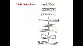
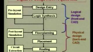
The optimization process is not a one-off task but spans several stages including:
- Floorplanning: The initial arrangement of functional blocks on the chip.
- Placement: The precise positioning of cells within the layout.
- Routing: Connecting the blocks with metal traces while minimizing interference.
- Post-placement optimizations: Adjustments made after the original placement to enhance performance further.
This chapter provides a deep dive into the various optimization strategies employed at each of these stages, tackling methods to improve performance, reduce power usage, and meet area constraints. By understanding and applying these strategies, designers can create VLSI layouts that are not only functional but also optimized for efficiency.
Youtube Videos
Audio Book
Dive deep into the subject with an immersive audiobook experience.
Overview of Physical Design
Chapter 1 of 4
🔒 Unlock Audio Chapter
Sign up and enroll to access the full audio experience
Chapter Content
Physical design in VLSI focuses on creating a functional and efficient layout of the circuit on the chip.
Detailed Explanation
Physical design is the process of arranging all the components of a circuit on a silicon chip. This involves considering how to place individual components (like transistors and wires) so that the circuit works correctly and efficiently. Key considerations include ensuring that these components can communicate properly and that they fit within the physical space available on the chip.
Examples & Analogies
Think of physical design like arranging furniture in a small room. You need to place items (like a sofa, table, and chairs) in a way that makes the room functional and easy to navigate while making sure everything fits without overcrowding.
Goals of Optimization Strategies
Chapter 2 of 4
🔒 Unlock Audio Chapter
Sign up and enroll to access the full audio experience
Chapter Content
Optimization strategies in physical design aim to meet various design goals, such as minimizing area, reducing power consumption, improving timing performance, and ensuring manufacturability.
Detailed Explanation
Optimization strategies are employed to achieve specific goals during the design process. Minimizing area refers to using the least amount of chip space possible, which can lower manufacturing costs. Reducing power consumption is crucial for making devices last longer, especially in portable electronics. Improving timing performance ensures that signals travel through the circuit quickly enough for proper functionality. Lastly, manufacturability ensures that the design can be produced efficiently and effectively at a factory.
Examples & Analogies
Imagine preparing a meal where you're trying to use the smallest pot (minimizing area), use less gas (reducing power), finish cooking quickly (improving timing), and make sure it’s simple enough for anyone to replicate (ensuring manufacturability).
Stages of the Optimization Process
Chapter 3 of 4
🔒 Unlock Audio Chapter
Sign up and enroll to access the full audio experience
Chapter Content
The optimization process spans multiple stages, including floorplanning, placement, routing, and post-placement optimizations.
Detailed Explanation
The optimization process consists of several important stages. Floorplanning is where the overall layout of the circuit is planned out, deciding where major components will go. Placement involves arranging smaller components within the predefined areas. Routing is the process of connecting these components with wires. Finally, post-placement optimizations are adjustments made after placement to refine performance and ensure everything works together smoothly.
Examples & Analogies
Think of building a new house. First, you make a floor plan (floorplanning), then you decide where to put the furniture (placement). After that, you install wiring and plumbing to connect everything (routing). Finally, you might rearrange some furniture or decorations for better flow (post-placement optimizations).
Key Topics in Optimization
Chapter 4 of 4
🔒 Unlock Audio Chapter
Sign up and enroll to access the full audio experience
Chapter Content
This chapter explores the key optimization strategies employed at each stage of the physical design process, including methods for improving performance, reducing power consumption, and meeting area constraints.
Detailed Explanation
Throughout this chapter, various strategies will be discussed that address the specific needs of each optimization stage. Strategies might include techniques to speed up circuit functions, reduce the energy used by the design, and fit components into a smaller area without losing quality or functionality.
Examples & Analogies
Picture a car manufacturer trying to make a more efficient vehicle. They need to ensure the car is fast (improving performance), uses less fuel (reducing power consumption), and can be produced within a certain budget (meeting area constraints).
Key Concepts
-
Optimization process: A systematic approach to improving design parameters like area, power, and timing.
-
Goals of optimization: To minimize area, reduce power consumption, improve performance, and ensure manufacturability.
-
Stages of optimization: Includes floorplanning, placement, routing, and post-placement.
Examples & Applications
Using gate clustering to optimize the area without hampering performance in VLSI designs.
Applying power gating techniques to reduce leakage power during idle states of the chip.
Memory Aids
Interactive tools to help you remember key concepts
Rhymes
To design in a skilled way, / Keep area small, let power play.
Stories
Imagine a chef organizing their kitchen (floorplanning) before preparing a dish (placement) and finally serving it (routing) to ensure everything is efficient.
Memory Tools
Remember 'MOP' for Goals: Minimize area, Optimize power, Ensure manufacturability.
Acronyms
FOPR for Stages
Floorplanning
Optimization
Placement
Routing.
Flash Cards
Glossary
- Optimization
The process of making a system as effective or functional as possible.
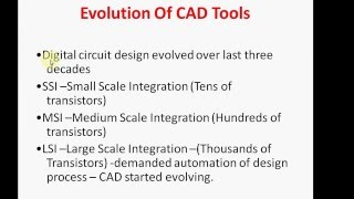
- VLSI
Very Large Scale Integration, a technology that allows thousands or millions of transistors to be integrated onto a single chip.
- Floorplanning
The arrangement of functional blocks on a chip.
- Placement
The positioning of individual cells in a design layout.
- Routing
The process of connecting cells with metal traces to establish electrical connections.
Reference links
Supplementary resources to enhance your learning experience.