
Timing-Driven Placement
Enroll to start learning
You’ve not yet enrolled in this course. Please enroll for free to listen to audio lessons, classroom podcasts and take practice test.
Interactive Audio Lesson
Listen to a student-teacher conversation explaining the topic in a relatable way.
Basics of Timing-Driven Placement
🔒 Unlock Audio Lesson
Sign up and enroll to listen to this audio lesson

Good morning, everyone! Today, we're discussing timing-driven placement in VLSI design. Can anyone share what they think this concept involves?

I think it has something to do with how we place the components based on their timing requirements.
Exactly! The main idea is to position the components—especially those along the critical paths—close together. This helps minimize delays. Can anyone tell me why it's essential to focus on critical paths?

Because they determine the maximum clock frequency?
Correct! Remember, optimizing timing helps meet the overall performance objectives of the VLSI design which affects its speed and efficiency.
Critical Paths and Their Impact
🔒 Unlock Audio Lesson
Sign up and enroll to listen to this audio lesson

Let's explore critical paths a bit more. Can anyone explain what makes a path critical?

It's the path with the longest delay, right? It influences the overall timing of the circuit.
Spot on! And if we reduce the delay in critical paths, what happens to the circuit?

The overall performance improves, and we can achieve higher clock speeds.
Great job, everyone! Remember, effective timing-driven placement is all about reducing delays along these paths for better functionality.
Balancing Act: Timing, Area, and Power
🔒 Unlock Audio Lesson
Sign up and enroll to listen to this audio lesson
Now let's talk about balancing timing with area and power. Who can explain why we need to create this balance?
If we focus too much on timing, we might use more area or power than allowed.
Exactly! It’s a balancing act. We must consider area usage and power consumption too. Can anyone think of a situation where this balance becomes critical?
In battery-powered devices, for instance, running low power would be crucial despite high-speed needs!
Well said! That reinforces why timing-driven placement is vital for high-performance yet efficient designs.
Introduction & Overview
Read summaries of the section's main ideas at different levels of detail.
Quick Overview
Standard
The concept of timing-driven placement revolves around placing cells strategically in a VLSI design to ensure that timing constraints are met. By positioning critical path components closer together, this technique aims to reduce signal delay and improve overall performance, thus striking a balance between area, power, and timing requirements.
Detailed
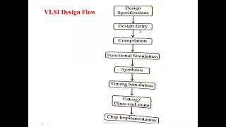
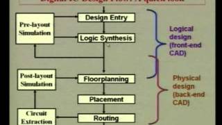
Timing-Driven Placement
Timing-driven placement is a crucial aspect of physical design in VLSI that optimally places circuit components based on timing requirements. The importance of this approach lies in its capability to enhance performance by minimizing delays along the critical paths. In a typical VLSI design, some paths are designated as 'critical'—these paths determine the maximum achievable clock frequency of the entire circuit.
In timing-driven placement, cells associated with these critical paths are positioned closer together to reduce the propagation delay through these paths, hence ensuring that timing constraints are satisfied. Moreover, this technique also involves analyzing the trade-offs between timing, area, and power consumption, aiming to achieve an efficient balance that meets the specifications of high-performance chips. By utilizing algorithms that incorporate timing analysis during the placement stage, designs can achieve improved performance metrics and ultimately lead to more successful VLSI implementations.
Youtube Videos
Audio Book
Dive deep into the subject with an immersive audiobook experience.
Optimizing Placement for Timing
Chapter 1 of 2
🔒 Unlock Audio Chapter
Sign up and enroll to access the full audio experience
Chapter Content
In this approach, placement is optimized based on the timing requirements of the design. Cells that are part of the critical path are placed closer to minimize delay, while less critical cells are placed in less constrained regions.
Detailed Explanation
Timing-driven placement focuses on arranging circuit elements (cells) in a way that meets specific timing requirements. The 'critical path' refers to the longest sequence of dependent tasks in a circuit that affects how fast it can operate. By placing essential components close together, the goal is to reduce delays in signal transmission.
For example, if you have a circuit where signal A needs to reach signal B quickly to function properly, placing A and B near each other on the chip can significantly decrease the time it takes for the signal to travel from A to B. Conversely, components that are less crucial can be positioned in areas that might be less optimal, allowing for a more efficient layout overall.
Examples & Analogies
Think of timing-driven placement like arranging a relay race team. If you have a runner who is the fastest but also needs to pass the baton quickly to the next runner, you want to make sure they are standing close to each other at the start. The faster they can pass the baton, the quicker the race will finish. Similarly, in circuit design, placing critical components close together speeds up performance just like well-coordinated runners in a relay.
Less Critical Cells Placement
Chapter 2 of 2
🔒 Unlock Audio Chapter
Sign up and enroll to access the full audio experience
Chapter Content
Cells that are part of the critical path are placed closer to minimize delay, while less critical cells are placed in less constrained regions.
Detailed Explanation
In timing-driven placement, distinguishing between critical and non-critical cells is crucial. Critical cells need to be placed in a manner that minimizes the distance signals have to travel, which, in turn, helps in lowering the overall delay of the circuit.
In contrast, less critical cells can be positioned further away from each other since their performance does not significantly affect the timing of the overall circuit. This approach helps to keep the design balanced and efficient, ensuring that important parts of the circuit are optimized without unnecessarily complicating the layout of less important components.
Examples & Analogies
Imagine arranging chairs in a big hall for a conference. You want key speakers (critical cells) to be seated close to each other so they can easily communicate, while attendees who don't need to interact with the speakers can sit further away and spread out. This arrangement ensures that the essential interactions happen quickly and smoothly—just like how critical cells in a circuit are placed for optimal timing.
Key Concepts
-
Timing-Driven Placement: A placement strategy focusing on the timing requirements of circuit paths to improve speed.
-
Critical Paths: The paths that determine the highest clock frequency of a circuit.
-
Timing Constraints: Rules that ensure signal timing meets operational requirements.
Examples & Applications
In a digital circuit design, if a flip-flop signal must propagate through several logic gates, placing those gates near each other will minimize the delay and satisfy the timing requirement.
In a chip design for a high-speed processor, the critical paths are identified, and the placement strategies are employed to ensure minimal distance between these critical components.
Memory Aids
Interactive tools to help you remember key concepts
Rhymes
In the race of circuits, speed we crave, / Place them right, that's how we save.
Stories
Imagine a relay race where the runner must pass the baton quickly to finish fastest. In VLSI design, if one runner (signal) has to run further (big delays), the race finishes slower. So, we place runners closer (timing-driven) for a speedy finish!
Memory Tools
To remember key steps: 'P.E.T.' – Place components, Evaluate delays, Test timing.
Acronyms
Remember 'T.E.C.' for Timing-Driven placement
Timing
Efficiency
Configuration.
Flash Cards
Glossary
- Critical Path
The longest path through the circuit, which determines the maximum frequency of operation.
- Timing Constraints
Limits on the maximum allowable delays in signal transmission that must be met for the circuit to operate correctly.
- Placement
The process of deciding where to physically locate the components of a circuit on a chip layout.
Reference links
Supplementary resources to enhance your learning experience.