
Optimization Strategies in Physical Design
Enroll to start learning
You’ve not yet enrolled in this course. Please enroll for free to listen to audio lessons, classroom podcasts and take practice test.
Interactive Audio Lesson
Listen to a student-teacher conversation explaining the topic in a relatable way.
Introduction to Optimization Strategies
🔒 Unlock Audio Lesson
Sign up and enroll to listen to this audio lesson

Today, we're diving into optimization strategies in physical design. Can anyone tell me why optimization is vital in designing VLSI circuits?

To make sure the circuit is efficient and functional?
Exactly! Optimization in physical design minimizes area, reduces power consumption, and improves timing. Think of it like packing a suitcase; the goal is to fit everything efficiently without wasting space!

What stages are involved in optimization?
Great question! The optimization process spans floorplanning, placement, routing, and even post-placement optimizations. Let’s explore these in detail in our next sessions.
Area Optimization Strategies
🔒 Unlock Audio Lesson
Sign up and enroll to listen to this audio lesson

Let’s talk about area optimization strategies. What’s one method to reduce chip area?

Cell sizing and resizing?
Correct! Adjusting cell sizes can either enhance performance or reduce area, depending on how we balance things. Remember, larger cells might improve speed but take up more space.

What about gate clustering? How does that help?
Great point! Gate clustering groups frequently used gates into smaller areas, minimizing space without sacrificing performance. It’s like keeping your tools close while you work.
Can you explain reuse of logic?
Sure! Reusing logic means sharing components between different parts of the design for similar functions, like using one tool for multiple purposes. Techniques like logic folding play a crucial role here.
Let’s recap: area optimization includes cell resizing, gate clustering, and logic reuse. Each method contributes to functional and smaller designs.
Power Optimization Strategies
🔒 Unlock Audio Lesson
Sign up and enroll to listen to this audio lesson
Now, let’s shift our focus to power optimization strategies. Who can tell me one method we use to reduce power consumption?
Clock gating?
Absolutely! Clock gating saves energy by turning off the clock to parts of the circuit when they're not in use. Think of it as turning off the lights in empty rooms.
What about power gating? How does that work?
Good question! Power gating completely shuts off power to inactive sections, effectively cutting down on leakage. It’s vital for battery-powered devices.
Is voltage scaling important?
Definitely! By adjusting voltage and frequency based on workload, we can optimize power consumption. It’s like adjusting your thermostat to save energy.
Quick summary: Power optimization includes techniques like clock gating, power gating, and voltage scaling. Each plays a vital role in managing energy use.
Timing and Routing Optimization
🔒 Unlock Audio Lesson
Sign up and enroll to listen to this audio lesson
Timing optimization is essential in ensuring circuits meet speed requirements. What’s the first step in timing optimization?
Optimizing the critical path?
Correct! The critical path determines maximum clock frequency. Reducing delays improves overall performance.
What is retiming?
Retiming involves shifting flip-flops to balance delays along the critical path. It's like redistributing weight to keep a balance when carrying something heavy.
How about routing optimization?
Routing optimization primarily focuses on wirelength minimization and congestion management. Shorter wires enhance speed and efficiency while reducing power.
Let’s summarize: Key strategies in timing include critical path optimization and retiming. In routing, we focus on wirelength and congestion management.
Advanced Optimization Techniques
🔒 Unlock Audio Lesson
Sign up and enroll to listen to this audio lesson
As designs grow more complex, we must explore advanced optimization techniques. Can anyone name one advanced strategy?
Genetic algorithms?
Exactly! Genetic algorithms mimic natural selection to tackle complex optimization problems, evolving solutions over generations.
What’s simulated annealing?
Simulated annealing is an iterative method that adjusts cell positions to minimize costs. It helps escape local minima, thanks to its strategy of accepting worse solutions under certain conditions.
Any other techniques?
Yes, particle swarm optimization simulates social behavior in nature to solve optimization problems efficiently.
To summarize, advanced techniques include genetic algorithms, simulated annealing, and particle swarm optimization. Each plays a crucial role in managing complexity.
Introduction & Overview
Read summaries of the section's main ideas at different levels of detail.
Quick Overview
Standard
Focusing on physical design within VLSI, this section delves into strategies aimed at optimization across four key areas: area, power, timing, and routing. Techniques such as clock gating, gate clustering, and critical path optimization are discussed to highlight their impact on performance and efficiency.
Detailed
Optimization Strategies in Physical Design
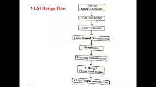
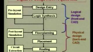
Physical design in VLSI revolves around creating a functional, efficient layout for circuits on chips. Various optimization strategies are implemented to achieve design goals such as minimizing area, reducing power consumption, improving timing performance, and ensuring manufacturability. This chapter presents key strategies employed at different stages in the physical design process, including:
Area Optimization
Area optimization strategies focus on reducing chip size while keeping functionality intact. Key techniques include:
- Cell Sizing and Resizing: Adjusting cell sizes affects both area and performance.
- Gate Clustering: Grouping frequently used gates minimizes area without performance loss.
- Floorplanning Optimization: Efficiently placing blocks reduces wirelength and routing congestion.
- Reuse of Logic: Sharing logic elements through techniques like logic folding and multiplexer sharing is critical.
Power Optimization
Power optimization is crucial for reducing energy consumption and heat. Strategies include:
- Clock Gating: Turns off clock to idle parts to reduce dynamism.
- Power Gating: Shuts off power supply to inactive circuit portions to cut leakage.
- Voltage Scaling: Adjusting voltage and frequency based on workload.
- MTCMOS: Utilizing transistors with varying threshold voltages for paths helps manage power effectively.
Timing Optimization
Ensuring designs meet timing constraints involves:
- Critical Path Optimization: Reducing delays in the critical path boosts performance.
- Retiming: Shifting flip-flops to balance delays.
- Pipelining: Introducing stages to enhance frequency but increases area.
- Clock Skew Optimization: Reducing clock signal arrival time differences.
Routing Optimization
Optimizing routing aids in achieving overall performance by:
- Wirelength Minimization: Short wires help lower delay and power.
- Congestion Management: Ensuring balanced wiring avoids delays and manufacturing issues.
- Multi-Layer Routing: Using several layers eases routing options.
- Timing-Driven Routing: Meeting timing constraints during layout.
Conclusion
Optimization strategies are foundational in modern VLSI design to ensure functional, efficient designs meeting area, power, timing, and manufacturability requirements.
Youtube Videos
Audio Book
Dive deep into the subject with an immersive audiobook experience.
Introduction to Optimization in Physical Design
Chapter 1 of 8
🔒 Unlock Audio Chapter
Sign up and enroll to access the full audio experience
Chapter Content
Physical design in VLSI focuses on creating a functional and efficient layout of the circuit on the chip. Optimization strategies in physical design aim to meet various design goals, such as minimizing area, reducing power consumption, improving timing performance, and ensuring manufacturability. The optimization process spans multiple stages, including floorplanning, placement, routing, and post-placement optimizations.
Detailed Explanation
In this introduction, we learn that physical design in VLSI (Very-Large-Scale Integration) is about arranging circuit components on a chip efficiently. There are several important goals for optimization—these include making the chip smaller (minimizing area), using less electricity (reducing power consumption), enhancing speed (improving timing performance), and ensuring that the chip can be manufactured easily (ensuring manufacturability). To achieve these goals, optimization involves several different steps, including how to layout the chip (floorplanning), where to place each component (placement), how to connect the components (routing), and making adjustments after placements are done (post-placement optimizations).
Examples & Analogies
Think of optimizing physical design like packing a suitcase for a trip. You want to fit all your clothes, shoes, and accessories into a limited space (the suitcase area) while making sure you can close it comfortably (ensuring functionality). You also want to make sure it’s not too heavy (reducing power consumption) as it may slow you down while traveling. The way you arrange everything matters—just like the different steps in optimization help to arrange the layout of a chip for best performance.
Area Optimization Strategies
Chapter 2 of 8
🔒 Unlock Audio Chapter
Sign up and enroll to access the full audio experience
Chapter Content
Area optimization focuses on reducing the chip's overall area while ensuring that the design remains functional. It is a critical aspect of VLSI design as it impacts the manufacturing cost, power consumption, and performance of the chip. Effective area optimization strategies can significantly improve the efficiency of the design.
Detailed Explanation
Area optimization is all about making the chip smaller while still keeping it functional. This is important because a smaller chip can be cheaper to produce, consume less power, and perform better. There are various strategies to achieve this, including adjusting the size of individual components (cell sizing and resizing), grouping related components together (gate clustering), efficiently arranging blocks on the chip (floorplanning optimization), and sharing similar functions between different parts of the design (reuse of logic). Each of these strategies plays a role in minimizing the overall area needed on the chip.
Examples & Analogies
Imagine trying to pack a tight space with boxes. You can make the boxes (cells) smaller or find ways to fit more into a single box by combining items (gate clustering). If you rearrange the items cleverly (floorplanning), you can potentially create more space. This is how engineers think about optimizing the physical space of a chip.
Power Optimization Strategies
Chapter 3 of 8
🔒 Unlock Audio Chapter
Sign up and enroll to access the full audio experience
Chapter Content
Power consumption is one of the most critical considerations in modern VLSI design. Power optimization reduces dynamic and static power consumption, prolongs battery life for mobile devices, and reduces heat dissipation in high-performance chips.
Detailed Explanation
Power optimization is crucial because modern devices require efficient energy use to function correctly and avoid overheating. Dynamic power consumption occurs when the device’s components are active, while static power consumption happens even when the device is idle. Power optimization techniques include clock gating (turning off clock signals when parts are not in use), power gating (shutting off power to inactive sections), voltage scaling (adjusting voltage based on demand), and using transistors strategically that can handle different voltage thresholds (multi-threshold CMOS). Each technique lowers power usage while trying to maintain device performance.
Examples & Analogies
Think of power optimization like managing a car’s fuel consumption. If you turn off the engine when idling (clock gating) or only turn on certain systems as needed (power gating), you save fuel. Similarly, adjusting how hard the engine works depending on the driving conditions (voltage scaling) helps maintain fuel efficiency. In this way, power optimization helps keep electronic devices running smoothly without wasting energy.
Timing Optimization Strategies
Chapter 4 of 8
🔒 Unlock Audio Chapter
Sign up and enroll to access the full audio experience
Chapter Content
Timing optimization ensures that the design meets the required timing constraints, such as setup time, hold time, clock skew, and propagation delays.
Detailed Explanation
Timing optimization focuses on meeting specific timing constraints necessary for correct circuit functionality. Key constraints include setup time (how long signals need to be stable before a clock edge), hold time (how long signals need to be stable after a clock edge), clock skew (the variance in clock signal arrival at flip-flops), and propagation delay (the time it takes for a signal to travel through a circuit). Techniques to achieve timing optimization include critical path optimization (reducing delays), retiming (shifting components to balance delays), pipelining (breaking long paths into smaller stages), and clock skew optimization (synchronizing clock signals). These strategies help the circuit function correctly and maximize performance.
Examples & Analogies
Imagine running a relay race, where each team member (circuit element) has to pass the baton (signal). If one runner is too slow in passing the baton (propagation delay) or if the team doesn’t coordinate well with their start times (clock skew), they risk losing the race. Timing optimization is like training the team to ensure every runner is at their best, minimizing the time between baton passes and ensuring precise timing to finish the race quickly.
Routing Optimization Strategies
Chapter 5 of 8
🔒 Unlock Audio Chapter
Sign up and enroll to access the full audio experience
Chapter Content
Routing is the process of connecting cells or blocks with metal traces. Optimizing routing improves the overall performance of the chip by minimizing wirelength, reducing congestion, and improving signal integrity.
Detailed Explanation
Routing optimization is critical in the design process, as it involves creating the necessary connections between components on a chip. Effective routing minimizes the lengths of these connections (wirelength) to reduce delays and power consumption, addresses congestion (too many connections in one area), and preserves signal integrity (ensuring the signal remains strong and clear). Strategies for routing optimization include wirelength minimization (finding the shortest paths), congestion management (evenly distributing connections), multi-layer routing (using several levels for connections), and timing-driven routing (considering timing in the layout).
Examples & Analogies
Think of routing optimization like planning a road trip. You want to take the shortest route (wirelength minimization) to your destination without getting stuck in traffic (congestion) and ensuring your vehicle delivery process keeps working smoothly (signal integrity). Just as you might choose to take different roads or even alternate routes based on current conditions, effective routing techniques help ensure the chip operates efficiently and successfully.
Placement and Routing Co-Optimization
Chapter 6 of 8
🔒 Unlock Audio Chapter
Sign up and enroll to access the full audio experience
Chapter Content
Placement and routing are closely related steps in physical design, and optimizing them together can yield better results. Co-optimization techniques ensure that the placement and routing decisions work together to minimize wirelength, improve timing, and reduce power consumption.
Detailed Explanation
Placement and routing are interconnected stages in chip design. By optimizing them together, efficiency can be significantly improved. Timing-driven placement focuses on placing key components, particularly those in the critical path, closer to one another to reduce delays. Similarly, power-aware placement and routing make sure to consider power needs while positioning components and laying out connections. This holistic approach ensures that adjustments in one area benefit the other, leading to an overall more efficient design.
Examples & Analogies
Consider organizing a community event where both seating (placement) and food stations (routing) need careful consideration. If you place the food stations near where people will most likely gather (timing-driven placement), it minimizes wait times and keeps the event flowing smoothly (improvement in timing and efficiency). By co-optimizing every element of the event, you make it enjoyable and efficient for everyone involved.
Advanced Optimization Techniques
Chapter 7 of 8
🔒 Unlock Audio Chapter
Sign up and enroll to access the full audio experience
Chapter Content
As VLSI designs continue to grow in complexity, advanced optimization techniques are employed to handle large designs with multiple constraints.
Detailed Explanation
With the increasing complexity of VLSI designs, more sophisticated optimization techniques are necessary. Advanced approaches such as genetic algorithms, which mimic natural selection, allow designers to navigate through vast design spaces and identify optimal solutions. Similarly, simulated annealing involves adjusting designs iteratively to find the best configuration while avoiding getting stuck in suboptimal solutions. Particle swarm optimization, inspired by group behavior in nature, further provides efficient solutions for complex problems. These methods help manage the multitude of constraints encountered in large designs, ensuring efficient and effective outcomes.
Examples & Analogies
Think of designing a complex video game. You would likely use multiple techniques to solve issues such as character designs, level layouts, and game mechanics. Just as game developers employ advanced algorithms and simulations to improve performance and resolve conflicts, engineers use sophisticated optimization techniques to ensure that intricate VLSI designs meet all their specific requirements efficiently.
Conclusion
Chapter 8 of 8
🔒 Unlock Audio Chapter
Sign up and enroll to access the full audio experience
Chapter Content
Optimization strategies in physical design are essential to meet the area, power, timing, and manufacturability requirements of modern VLSI circuits. From minimizing area and reducing power consumption to optimizing timing and routing, these strategies ensure that the design is both functional and efficient.
Detailed Explanation
In conclusion, optimization strategies play a crucial role in the physical design of VLSI circuits. By addressing key aspects such as area reduction, power efficiency, timing accuracy, and proper routing, these strategies help ensure that modern electronic devices are both effective in performance and feasible to manufacture. The importance of advanced algorithms is emphasized, as they provide solutions to the complexities involved in designing large-scale VLSI systems. Upcoming chapters will delve deeper into these strategies and their implementation in industry-standard tools.
Examples & Analogies
Just as a chef meticulously refines their recipes to achieve the best dish possible, engineers fine-tune various strategies to create the most efficient and functional VLSI designs. Each optimization step enhances the overall 'recipe' of the chip, ensuring it meets all the necessary requirements for excellent performance and manufacturability.
Key Concepts
-
Critical Path: The longest path through a circuit, determining the maximum clock frequency.
-
Clock Gating: A method to reduce dynamic power by turning off the clock to idle circuit parts.
-
Retiming: Adjusting the positions of flip-flops on the critical path to optimize timing.
-
Wirelength Minimization: A goal in routing to reduce delay and power consumption.
Examples & Applications
Using clock gating, a VLSI design can conserve power by shutting off unused sections, making it ideal for battery-powered devices.
Applying gate clustering reduces layout area by consolidating frequently used gates, enhancing performance.
Memory Aids
Interactive tools to help you remember key concepts
Rhymes
To save on space, we must embrace, sizes and clusters in manageable place.
Stories
Imagine you are packing a suitcase. You put together items you will use frequently so they're easy to grab. This is like gate clustering, where we group logic gates together to save space.
Memory Tools
APPT – Area, Power, Performance, Timing – the key optimization areas we explore.
Acronyms
RCP - Reduce Circuit Power – a reminder for power optimization techniques.
Flash Cards
Glossary
- VLSI
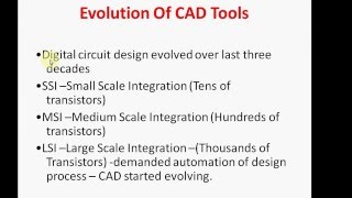
Very Large Scale Integration, a process of creating integrated circuits by combining thousands of transistors into a single chip.
- Floorplanning
The arrangement of blocks on a chip to optimize performance or area.
- Gate Clustering
Grouping logic gates that are frequently used together to minimize layout area.
- Clock Gating
A power optimization technique that turns off the clock to portions of a circuit when they are not in use.
Reference links
Supplementary resources to enhance your learning experience.