
Floorplanning Optimization
Enroll to start learning
You’ve not yet enrolled in this course. Please enroll for free to listen to audio lessons, classroom podcasts and take practice test.
Interactive Audio Lesson
Listen to a student-teacher conversation explaining the topic in a relatable way.
Introduction to Floorplanning Optimization
🔒 Unlock Audio Lesson
Sign up and enroll to listen to this audio lesson

Today, we'll dive into floorplanning optimization. Why do you all think it's essential in VLSI design?

Is it because it helps to save space on the chip?
Exactly, saving space is crucial! Efficient floorplanning can lead to reduced wirelength, which minimizes routing congestion. Can anyone tell me a consequence of increased wirelength?

Increased delay and possibly more power consumption?
Correct! And remember, less congestion also improves timing performance. Think of it as traffic management on a road—less congestion translates to better flow.

So, how do we decide where to place each block?
Great question! Placement depends on the functionality of the blocks and their interconnections. A good guideline is to keep frequently interacting blocks close together.

That makes sense; so it’s about minimizing distance?
Exactly! Minimizing distances leads to efficient designs. In summary, floorplanning optimization not only saves space but significantly enhances circuit performance.
Techniques for Floorplanning Optimization
🔒 Unlock Audio Lesson
Sign up and enroll to listen to this audio lesson

Now let’s discuss some techniques for effective floorplanning optimization. Can anyone mention a technique?
What about clustering related logic gates?
Exactly! Gate clustering is key. By grouping gates that function together, we minimize area without sacrificing overall performance. What else can be considered?
Adjusting the size of the cells that contain the gates?
Yes! Cell sizing can also help optimize area, but it’s a balancing act between size and performance. Does anyone remember the trade-offs involved?
Bigger cells could improve speed but increase area.
Absolutely right! Balancing these factors is crucial for achieving the most efficient layout. Let’s summarize today: good floorplanning techniques should minimize area while considering performance and timing.
Challenges in Floorplanning Optimization
🔒 Unlock Audio Lesson
Sign up and enroll to listen to this audio lesson
Lastly, let’s address some challenges in floorplanning optimization. What kind of challenges do you think designers face?
Maybe the conflicts between area and performance?
Very insightful! Additionally, designers deal with complex interconnect requirements and timing constraints that can complicate floorplanning.
That sounds like a tough balancing act!
It truly is. Designing a floorplan requires iterative adjustments and optimization techniques. Remember, a well-optimized floorplan is the backbone of a successful VLSI chip design.
So it's not just about fitting everything in, but making it work effectively too?
Exactly! Keeping performance high while optimizing area is the essence of floorplanning optimization. Today, you’ve grasped the importance and techniques of optimization in VLSI design.
Introduction & Overview
Read summaries of the section's main ideas at different levels of detail.
Quick Overview
Standard
This section discusses the significance of floorplanning optimization in VLSI design, emphasizing how efficient arrangement of blocks can lead to reduced wirelength, minimized routing congestion, and overall area reduction, which are critical for achieving effective chip layout and performance.
Detailed
Detailed Summary of Floorplanning Optimization
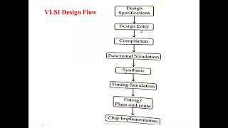
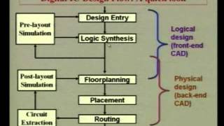
Floorplanning optimization is a vital aspect of VLSI physical design focusing on the strategic layout of circuit blocks on a chip. The aim of floorplanning is to efficiently position these blocks to minimize wirelength and routing congestion, both of which are essential for enhancing performance while reducing overall chip area. An effective floorplan not only contributes to area savings but also plays a crucial role in ensuring manufacturability and improving timing performance. Factors encompassed in the optimization process include the arrangement of logic cells and the hierarchical efficiencies achieved through systematic block positioning. By understanding the principles behind effective floorplanning, designers can achieve significant improvements in VLSI circuit design.
Youtube Videos

Audio Book
Dive deep into the subject with an immersive audiobook experience.
Role of Floorplanning in Area Optimization
Chapter 1 of 3
🔒 Unlock Audio Chapter
Sign up and enroll to access the full audio experience
Chapter Content
Floorplanning plays a significant role in area optimization. Placing blocks efficiently on the chip reduces wirelength and minimizes routing congestion, which can contribute to area reduction.
Detailed Explanation
Floorplanning refers to the arrangement of the various components (or blocks) of a chip design on the silicon surface. By strategically placing these blocks, designers can reduce the total distance that wires need to travel between them. This not only decreases the overall size of the chip but also helps to minimize potential routing issues. Efficient floorplanning leads to shorter wires, which improves performance and makes the manufacturing process easier.
Examples & Analogies
Imagine you're organizing a small office with several desks for employees. If you place the desks too far apart from each other, employees will waste time walking back and forth to communicate. However, if you group team members who frequently collaborate together and place their desks closer, not only do you save space, but you also enhance their productivity due to reduced travel distance. Similarly, good floorplanning in chip design optimizes the placement for efficiency and performance.
Impact of Wirelength on Performance
Chapter 2 of 3
🔒 Unlock Audio Chapter
Sign up and enroll to access the full audio experience
Chapter Content
The efficient placement of blocks leads to reduced wirelength, which is crucial for improving timing performance and minimizing signal delays.
Detailed Explanation
Wirelength refers to the total length of the electrical connections (wires) that link different blocks on a chip. Longer wires introduce delay because signals take time to travel between components. When blocks are placed too far apart, the wires that connect them need to be longer, causing delays in signal transmission. This can adversely affect the overall performance of the circuit by slowing down operations. Thus, careful placement to minimize wirelength directly contributes to faster signal processing.
Examples & Analogies
Think of a relay race where runners pass a baton. If the runners are positioned too far apart, the baton takes longer to reach the next runner, slowing down the overall time. In the same way, reducing wirelength ensures that data travels quickly between components in a chip, thus improving overall performance and efficiency.
Minimizing Routing Congestion
Chapter 3 of 3
🔒 Unlock Audio Chapter
Sign up and enroll to access the full audio experience
Chapter Content
Efficient floorplanning also minimizes routing congestion, which is essential to ensure that signals can pass through the chip without delay or interference.
Detailed Explanation
Routing congestion occurs when too many wires try to occupy the same area on the chip, leading to physical overlaps and signal interference. This is especially problematic as it can result in slower operation or failures in signal integrity. By optimizing the floorplan, designers can distribute components and their associated connections more evenly, thus reducing congestion. This ensures that signals flow smoothly across the chip without unnecessary delays that could affect performance.
Examples & Analogies
Picture a busy city intersection where too many cars converge at the same time. If the street layout is poor, traffic becomes congested and cars get delayed. However, if the roads are well-planned and cars are directed smoothly without overlapping routes, traffic flows more freely and efficiently. Likewise, reducing routing congestion in chip design allows signals to traverse the circuit without hitting 'traffic jams', thereby enhancing overall efficiency and performance.
Key Concepts
-
Floorplanning: The strategic arrangement of blocks within a chip.
-
Wirelength: A critical factor affecting chip performance due to interconnections.
-
Congestion: A condition that arises from excessive wiring in specific chip areas.
-
Gate Clustering: An optimization technique for space-saving.
-
Cell Sizing: The modification of gate sizes impacting area and speed.
Examples & Applications
In a complex chip design, grouping related functionalities into clusters can reduce total area and improve interconnect efficiency.
When designing a processor, placing frequently communicating components close together can enhance performance and reduce timing delays.
Memory Aids
Interactive tools to help you remember key concepts
Rhymes
Floorplan and design go hand in hand, optimizing space is the goal that's planned.
Stories
Imagine a busy city (a chip) where blocks (buildings) need to be arranged for quick travel (signals). A well-planned layout reduces traffic (congestion) and saves time (performance).
Memory Tools
For remembering optimization techniques, think 'GCCS': Gate Clustering, Cell Sizing, Congestion management, and Sequencing.
Acronyms
In memory of Floorplanning, use 'SAVE'
Space
Arrangement
Value
Efficiency.
Flash Cards
Glossary
- Floorplanning
The process of arranging circuit blocks on a chip to optimize area and performance.
- Wirelength
The total length of wires needed to connect circuit components, impacting performance and power consumption.
- Congestion
A condition where too many connections are made within a given area, potentially leading to delays.
- Gate Clustering
A technique to group together logic gates that are frequently used to reduce area without compromising functionality.
- Cell Sizing
The adjustment of cell sizes which can influence both performance and area.
Reference links
Supplementary resources to enhance your learning experience.